TIDT199A January 2021 – December 2022
2.4 Current Limit
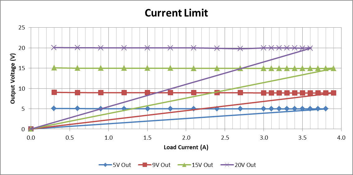
The following image illustrates the current limit graph for this design.
 Figure 2-7 Current Limit
TIDT199A January 2021 – December 2022
The following image illustrates the current limit graph for this design.
 Figure 2-7 Current Limit