TIDT205 February   2021


  1. 1Description
  2. 2Test Prerequisites
    1. 2.1 Voltage and Current Requirements
    2. 2.2 Considerations
    3. 2.3 Dimensions
  3. 3Testing and Results
    1. 3.1 Efficiency Graphs
    2. 3.2 Efficiency Data
    3. 3.3 Load Regulation
    4. 3.4 Thermal Image
    5. 3.5 Bode Plots
    6. 3.6 Conducted Emissions Testing (CISPR 25, Class 5)
  4. 4Waveforms
    1. 4.1 Switching
    2. 4.2 Output Voltage Ripple
    3. 4.3 Load Transients
    4. 4.4 Start-up Sequence
    5. 4.5 Termination Sequence

Switching

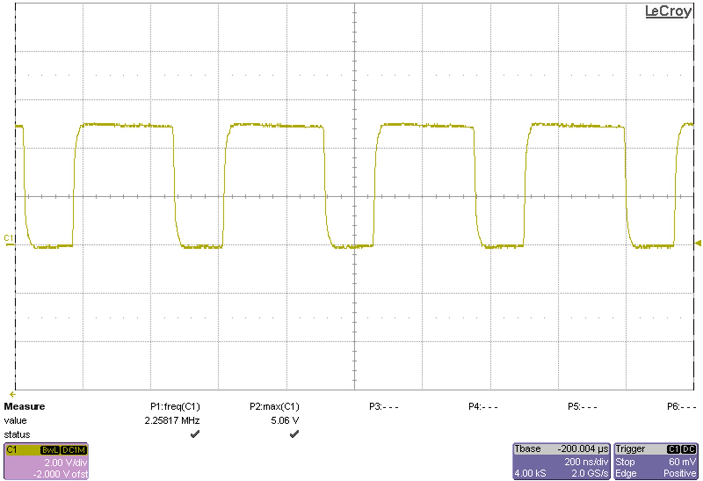
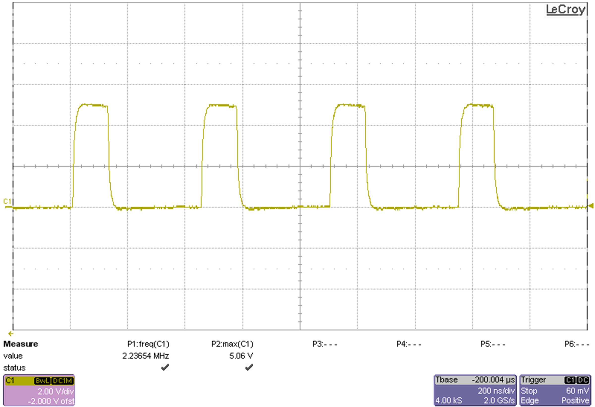
The switch node measurements are shown in the follwing images. The board was supplied with 13.5 VIN in all cases.
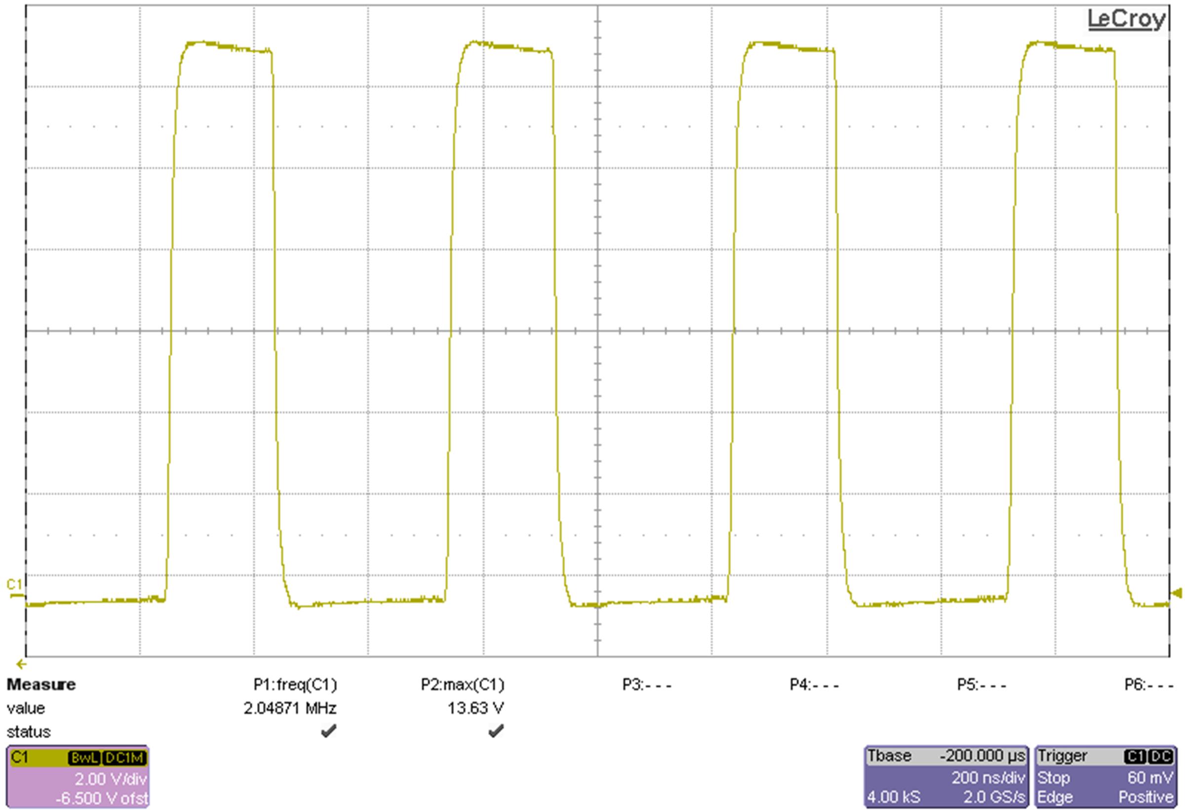
GUID-20210205-CA0I-CDFD-LNXX-GRNFF553WHMW-low.jpgFigure 4-1 5-V Rail Switch Node
GUID-20210205-CA0I-QDQC-VNHB-NXGWWR1VGMKJ-low.jpgFigure 4-3 1.8-V Rail Switch Node
GUID-20210205-CA0I-VRBV-JV8Z-4GB9SRHZVCHQ-low.jpgFigure 4-5 1.175-V Rail Switch Node
GUID-20210205-CA0I-KZX5-09BV-2KVX7LWGRXZP-low.jpgFigure 4-2 3.3-V Rail Switch Node
GUID-20210205-CA0I-X3SF-WCHM-TZ88VLGLQ48N-low.jpgFigure 4-4 1.35-V Rail Switch Node