TIDT222 April   2021


  1. 1Description
  2. 2Test Prerequisites
    1. 2.1 Voltage and Current Requirements
    2. 2.2 Required Equipment
    3. 2.3 Considerations
    4. 2.4 Dimensions
    5. 2.5 Test Setup
  3. 3Testing and Results
    1. 3.1 Efficiency and Loss Graphs
    2. 3.2 Efficiency Data
    3. 3.3 Thermal Images
    4. 3.4 Bode Plots
  4. 4Waveforms
    1. 4.1 Switching
    2. 4.2 Output Voltage Ripple
    3. 4.3 Load Transients
    4. 4.4 Start-up Sequence

Start-up Sequence

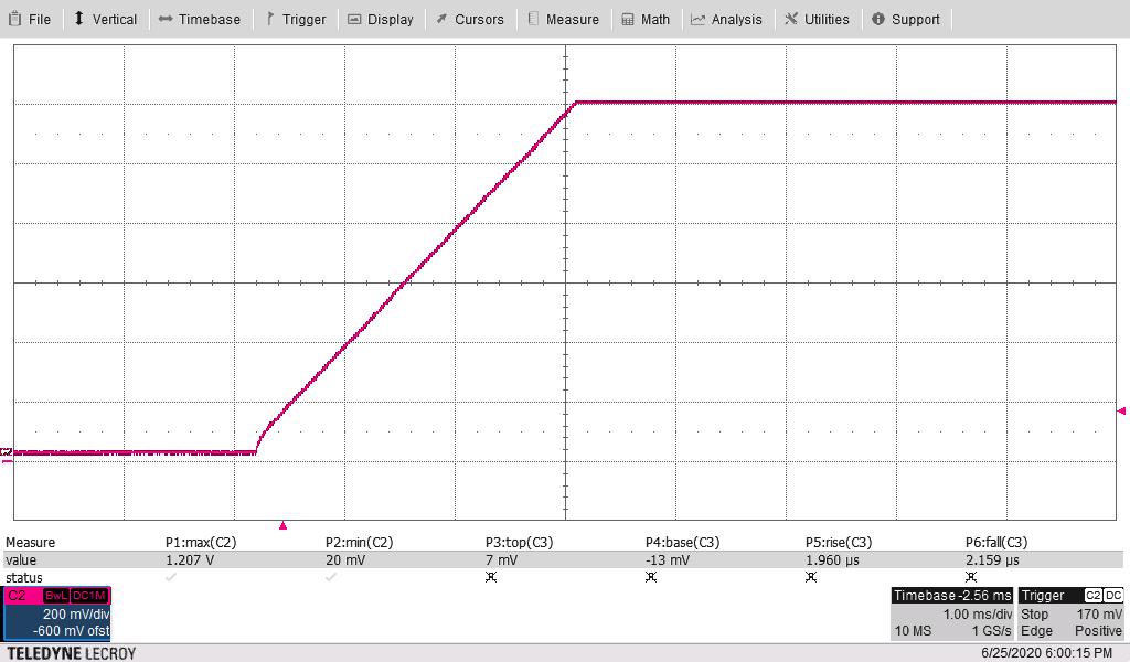
Figure 4-13 shows the output voltage startup waveform after the application of 12 V in and the Enable pin manually disconnected from GND with the 1.2-V output loaded to 0 A.

The faster 36-kHz bandwidth loop set by NVM is used here, as faster loops have greater risk of turn on overshoot.
GUID-20210105-CA0I-LJHQ-T88F-H9XMHV2M08K7-low.jpg
200 mV/DIV, 1 ms/DIV
Figure 4-13 Start-Up Waveform