TIDT226 April   2021


  1. 1Description
  2. 2Test Prerequisites
    1. 2.1 Voltage and Current Requirements
    2. 2.2 Required Equipment
  3. 3Testing and Results
    1. 3.1 Thermal Images
    2. 3.2 Efficiency and Power Dissipation Graph
    3. 3.3 Efficiency and Power Dissipation Data
    4. 3.4 Cross-Load Voltage Regulation
    5. 3.5 Voltage Regulation Graph
  4. 4Waveforms
    1. 4.1 Start-up Sequence
    2. 4.2 Switch Node
    3. 4.3 Output Voltage Ripple
    4. 4.4 Load Transients

Switch Node

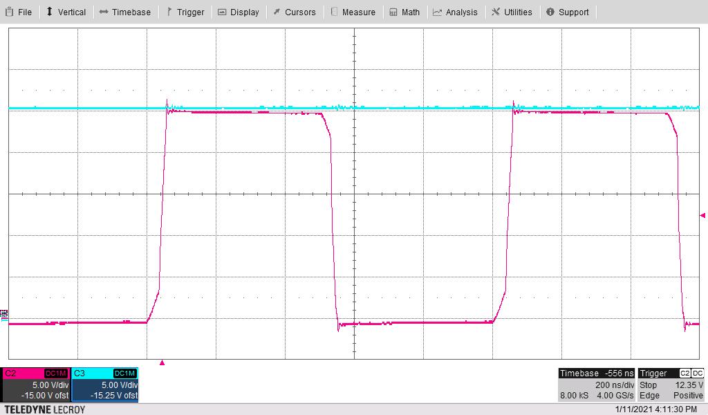
The following waveform shows the primary-side switch node voltage (Red) at TP5 and the total rectified secondary output voltage (Blue). The input voltage is 24 V and the 20-V and –4-V outputs are loaded to 0 mA each.
GUID-20210219-CA0I-DGH8-6DPW-83WNPGVXZHKP-low.jpg
5 V/div, 200 ns/div, 750 MHz BWL
Figure 4-5 Primary-Side Switch Node Voltage and Total Rectified Secondary Output Voltage

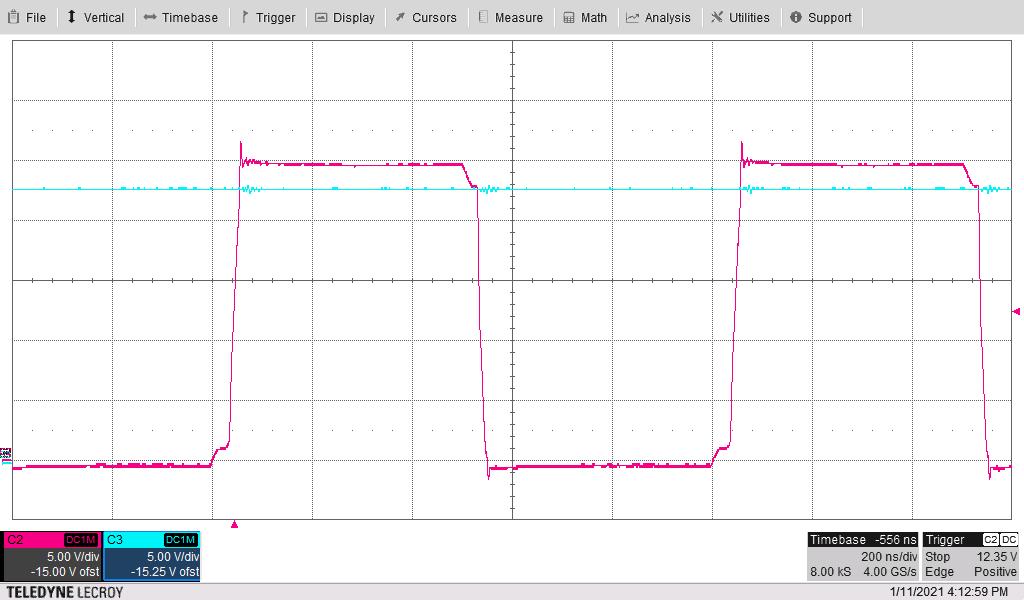
The following waveform shows the primary-side switch node voltage (Red) at TP5 and the total rectified secondary output voltage (Blue). The input voltage is 24 V and the 20-V and –4-V outputs are loaded to 100 mA each.
GUID-20210219-CA0I-G81R-T4FR-DRCVJHQRNBJZ-low.jpg
5 V/div, 200 ns/div, 750 MHz BWL
Figure 4-6 Primary-Side Switch Node Voltage and Total Rectified Secondary Output Voltage

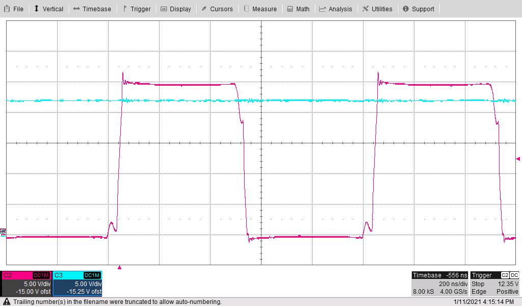
The following waveform shows the primary-side switch node voltage (Red) at TP5 and the total rectified secondary output voltage (Blue). The input voltage is 24 V and the 20-V and –4-V outputs are loaded to 200 mA each.
GUID-20210219-CA0I-7X7K-SX1F-RJ1LHJZTFDC3-low.jpg
5 V/div, 200 ns/div, 750 MHz BWL
Figure 4-7 Primary-Side Switch Node Voltage and Total Rectified Secondary Output Voltage

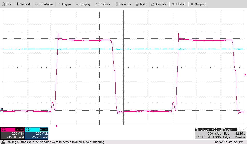
The following waveform shows the primary-side switch node voltage (Red) at TP5 and the total rectified secondary output voltage (Blue). The input voltage is 24 V and the 20-V and –4-V outputs are loaded to 300 mA each.
GUID-20210219-CA0I-P82P-2FVX-5CH2FHCWCNGM-low.jpg
5 V/div, 200 ns/div, 750 MHz BWL
Figure 4-8 Primary-Side Switch Node Voltage and Total Rectified Secondary Output Voltage

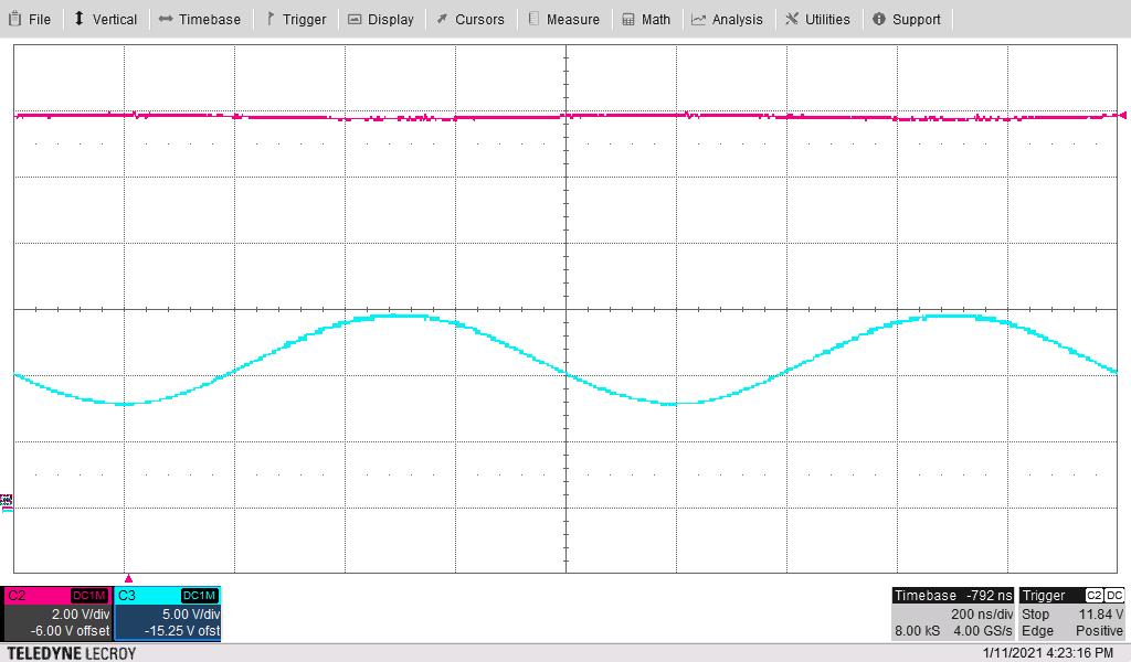
The following waveform shows the voltage at the middle of the input capacitor divider at C2 and C9 (Red) and the secondary rectified voltage across C3 (Blue). The input voltage is 24 V and the 20-V and –4-V outputs are loaded to 100 mA each.
GUID-20210219-CA0I-DKHM-600T-FXL8MVPVNWQ1-low.jpg
C2/C9: 2 V/div, C3: 5 V/div, 200 ns/div, 750 MHz BWL
Figure 4-9 Input Capacitor Divider Voltage and Secondary Rectified Voltage

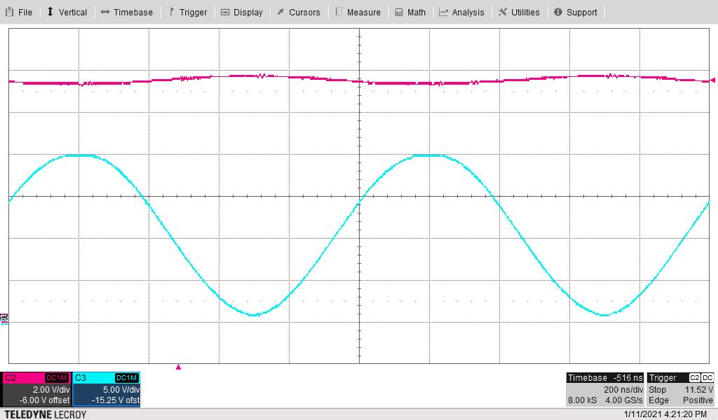
The following waveform shows the voltage at the middle of the input capacitor divider at C2 and C9 (Red) and the secondary rectified voltage across C3 (Blue). The input voltage is 24 V and the 20-V and –4-V outputs are loaded to 300 mA each.
GUID-20210219-CA0I-J2DS-3CGV-TVGSRVZC7GMB-low.jpg
C2/C9: 2 V/div, C3: 5 V/div, 200 ns/div, 750 MHz BWL
Figure 4-10 Input Capacitor Divider Voltage and Secondary Rectified Voltage