TIDT236 March 2022 TPS7H1101A-SP
3.4 Start-up Sequence
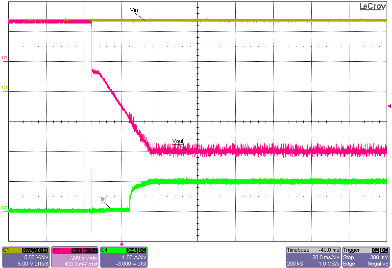
Figure 3-11 to Figure 3-18 show the output voltage start-up waveforms at 12-V input and –0.2-V and –0.6-V output with the converter starting up into no load and into 15-A constant-current load using the electronic load. It can be seen that just before start-up, the output voltage actually reaches approximately +0.25 V. This is due to the bias currents passing through the regulator IC and onward through the clamping Schottky diode, D1. If this diode was not placed there, then the bias current would have passed through the body diode of the low-side FET of the regulator and generated an even higher voltage at the –VOUT connection. This inherent behavior is due to the inverting buck-boost topology and how the IC GND is actually floating initially, before regulation ensues. The two methods of enabling the converter have been captured: one where the input voltage is turned ON and the converter waits for the Enable signal to go HIGH; the other where the Enable signal is already set HIGH and the converter waits for the main power supply to be turned ON.
 Figure 3-11 Start-up Into No Load, 12-V Input, –0.2-V
Output, Start-up Initiated via the Enable Connection (Input Supply Already
Turned ON)
 Figure 3-12 Start-up Into 15-A Constant-Current Load, 12-V
Input, –0.2-V Output Start-up Initiated via the Enable Connection (Input Supply
Already Turned ON)
 Figure 3-13 Start-up Into No Load, 12-V Input, –0.2-V
Output, Start-up Initiated via Input Supply (Enable Signal Already Set
High)
 Figure 3-14 Start-up Into 15-A Constant-Current Load, 12-V
Input, –0.2-V Output, Start-up Initiated via Input Supply (Enable Signal Already
Set High)
 Figure 3-15 Start-up Into No Load, 12-V Input, –0.6-V
Output, Start-up Initiated via the Enable Connection (Input Supply Already
Turned ON)
 Figure 3-16 Start-up Into 15-A Constant-Current Load, 12-V
Input, –0.6-V Output, Start-up Initiated via the Enable Connection (Input Supply
Already Turned ON)
 Figure 3-17 Start-up Into No Load, 12-V Input, –0.6-V
Output, Start-up Initiated via Input Supply (Enable Signal Already Set
High)
 Figure 3-18 Start-up Into 15-A Constant-Current Load, 12-V
Input, –0.6-V Output, Start-up Initiated via Input Supply (Enable Signal Already
Set High)