TIDT252 December 2021
3.4 Load Transients
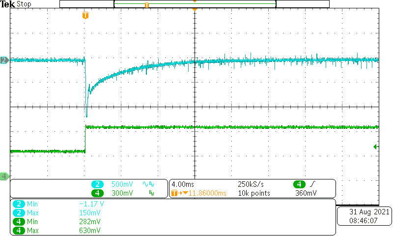
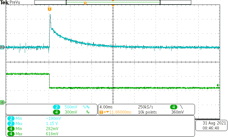
Load transient response waveforms are shown in Figure 3-5 and Figure 3-6.

Ch2: AC-coupled output voltage at
12.0 VIN, bw limited (20 MHz) [scale: 500 mV/div, 4.0 ms/div]
Ch4: Load transient from 30.0 A to
60.0 A, slew rate 1.0 A/μs [scale: 30.0 A/div, 4.0 ms/div]
Figure 3-5 Load Transient - Rising
Edge
Ch2: AC-coupled output voltage at
12.0 VIN, bw limited (20 MHz) [scale: 500.0 mv/div, 4.0
ms/div]
Ch4: Load transient from 60.0 A to
30.0 A, slew rate 1 A/μs [scale: 30.0 A/div, 4.0 ms/div]
Figure 3-6 Load Transient - Falling
Edge