TIDT264 March   2022


  1.   Description
  2.   Features
  3.   Applications
  4. 1Test Prerequisites
    1. 1.1 Voltage and Current Requirements
    2. 1.2 Required Equipment
    3. 1.3 Considerations
    4. 1.4 Dimensions
  5. 2Testing and Results
    1. 2.1 Efficiency Graphs
    2. 2.2 Efficiency Data
    3. 2.3 Thermal Images
    4. 2.4 EMI
  6. 3Waveforms
    1. 3.1 Switching
    2. 3.2 Output Voltage Ripple
    3. 3.3 Load Transients

Switching

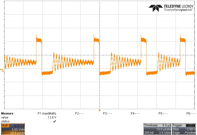
Switching behavior is shown in the following figures. The switching node in Figure 3-1 is measured across Vs to GND and the second switching node shown in Figure 3-2 is measured across D5. The maximum stress is found across the primary switching node at 395 V.
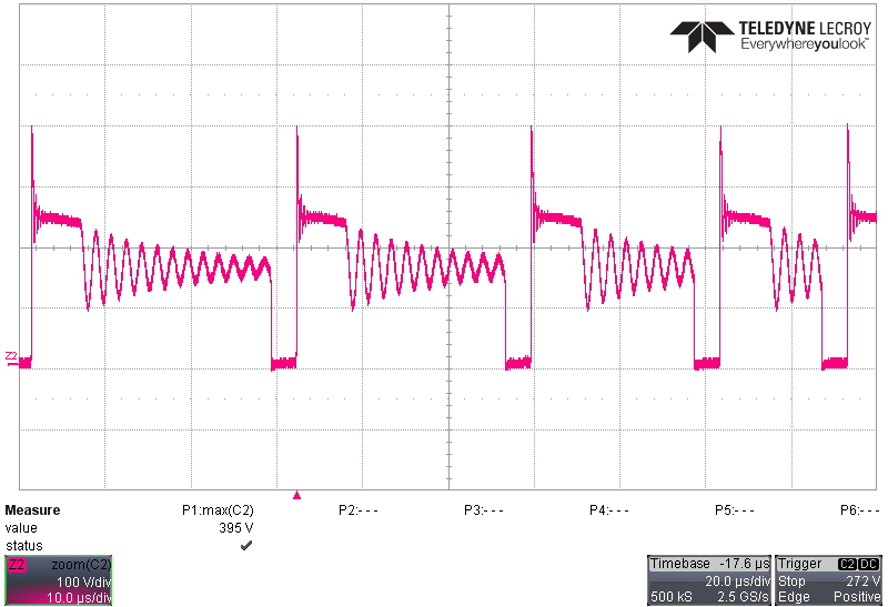
GUID-20220302-SS0I-F2XM-LBPR-DRL9MZJ3Z4GF-low.jpg Figure 3-1 Switching 1
GUID-20220302-SS0I-FBBL-XGK7-DTBX8DTWWN28-low.jpg Figure 3-2 Switching 2