TIDT274 April   2022


  1.   Description
  2.   Features
  3.   Applications
  4. 1Test Prerequisites
    1. 1.1 Voltage and Current Requirements
    2. 1.2 Considerations
    3. 1.3 Dimensions
  5. 2Testing and Results
    1. 2.1 Efficiency Graphs
    2. 2.2 Load Regulation
    3. 2.3 Thermal Images
    4. 2.4 Bode Plots
  6. 3Waveforms
    1. 3.1 Switching
      1. 3.1.1 Switchnode to GND
      2. 3.1.2 Switchnode to –VOUT
    2. 3.2 Input Voltage Ripple
    3. 3.3 Output Voltage Ripple
    4. 3.4 Load Transients
    5. 3.5 Start-Up Sequence
    6. 3.6 Shutdown Sequence

Bode Plots

The bode plot is shown in the following figure.
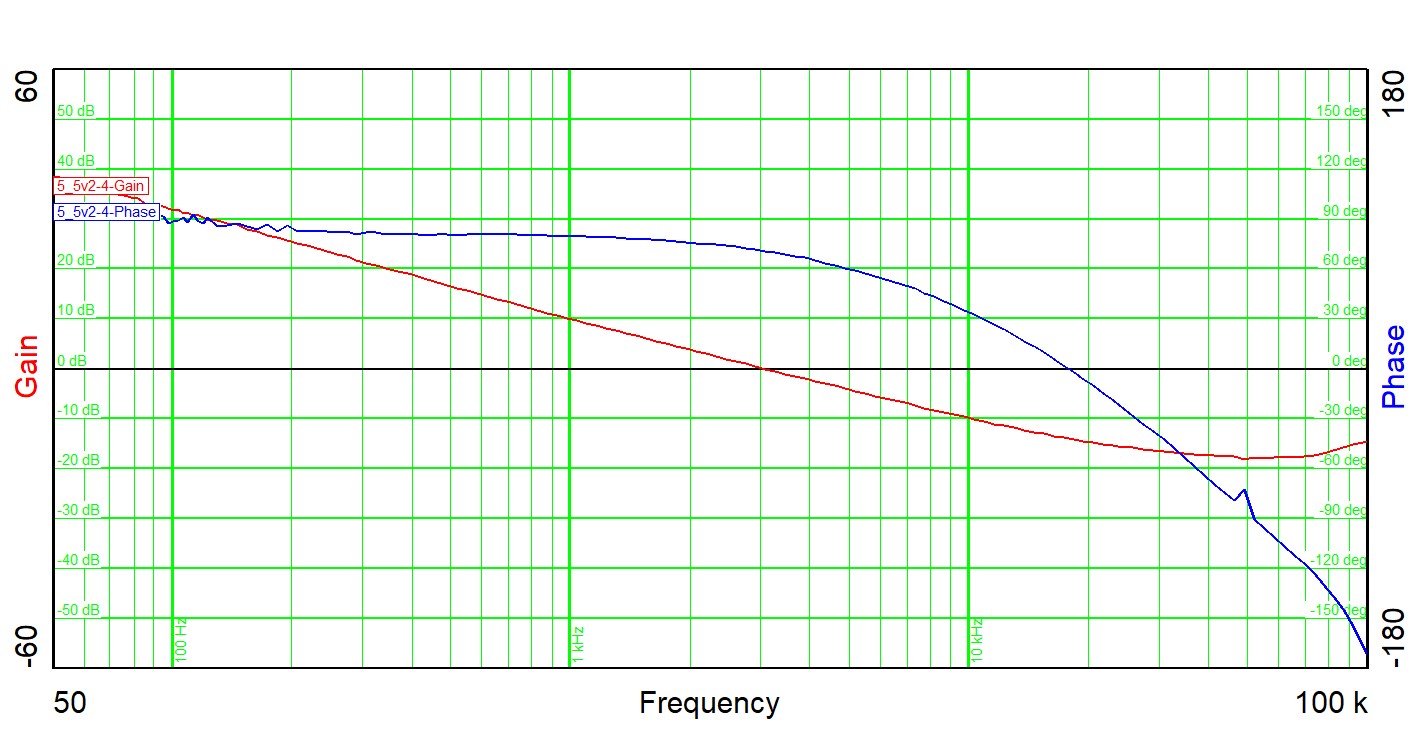
GUID-20220401-SS0I-SHVW-43SS-6TMZ2L25MHGX-low.jpgFigure 2-4 Control Loop Frequency Response
VIN 5.2 V
Bandwidth (kHz) 3
Phase Margin 70.7°
Slope (20 dB / decade) –0.95
Gain Margin (dB) –14
Slope (20 dB / decade) –0.73
Freq (kHz) 17.8