TIDT278
April 2022
Description
Features
Applications
1
Test Prerequisites
1.1
Voltage and Current Requirements
1.2
Considerations
1.3
Dimensions
2
Testing and Results
2.1
Efficiency Graphs
2.2
Loss
2.3
Load Regulation
2.3.1
5-V Output Voltage
2.3.2
3.3-V Output Voltage
2.3.3
12-V Output Voltage
2.4
Line Regulation
2.4.1
5-V Outputs
2.4.2
3.3-V Output Voltage
2.4.3
12-V Output Voltage
2.4.4
Efficiency and Loss in Dependance of Input Voltage
2.5
Cross Regulation Light Load and Full Load
2.5.1
Bias Current 1 mA
2.5.2
Bias Current 5 mA
2.6
Thermal Images
2.7
Bode Plots
3
Waveforms
3.1
Switching
3.1.1
Q1 Drain to GND
3.1.2
Q1 Gate to GND
3.1.3
D1 Anode to 12 VOUT
3.2
Input Voltage Ripple
3.3
Output Voltage Ripple
3.3.1
5-V Output Voltage (Primary)
3.3.2
5-V Output Voltage (Secondary)
3.3.3
3.3-V Output Voltage
3.3.4
12-V Output Voltage
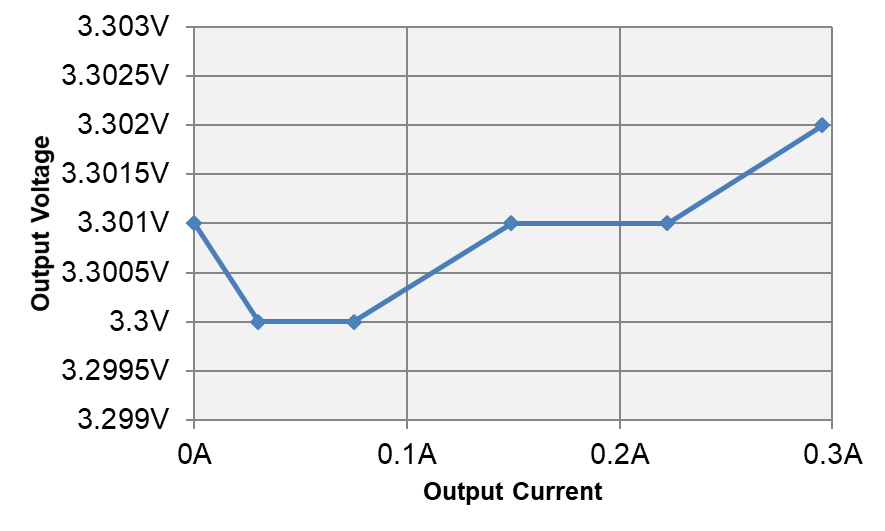
2.3.2
3.3-V Output Voltage
Figure 2-5
Output Voltage vs Output Current
Note:
Figure 2-6
illustrates
LDO inputs
at 3.3 V.
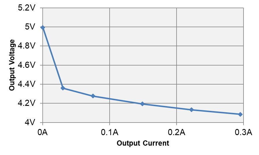
Figure 2-6
Voltage at 3.3-V LDO Input vs Output Current