TIDT280 May   2022


  1.   Description
  2.   Features
  3.   Applications
  4. 1Test Prerequisites
    1. 1.1 Voltage and Current Requirements
    2. 1.2 Considerations
    3. 1.3 Dimensions
  5. 2Testing and Results
    1. 2.1 Efficiency
    2. 2.2 Loss
    3. 2.3 Load Regulation
    4. 2.4 Line Regulation
    5. 2.5 Thermal Images
    6. 2.6 Bode Plots
      1. 2.6.1 9-V Input Voltage
      2. 2.6.2 24-V Input Voltage
      3. 2.6.3 48-V Input Voltage
      4. 2.6.4 56-V Input Voltage
  6. 3Waveforms
    1. 3.1 Switching
      1. 3.1.1 Transistor Q5 (Low-Side FET)
        1. 3.1.1.1 Drain - Source
          1. 3.1.1.1.1 9-V Input Voltage
          2. 3.1.1.1.2 56-V Input Voltage
        2. 3.1.1.2 Gate - Source
          1. 3.1.1.2.1 9-V Input Voltage
          2. 3.1.1.2.2 56-V Input Voltage
      2. 3.1.2 Transistor Q1 (High-Side FET)
        1. 3.1.2.1 Source - Drain (Referenced to VIN)
          1. 3.1.2.1.1 9-V Input Voltage
          2. 3.1.2.1.2 56-V Input Voltage
        2. 3.1.2.2 Gate - Source
          1. 3.1.2.2.1 9-V Input Voltage
          2. 3.1.2.2.2 56-V Input Voltage
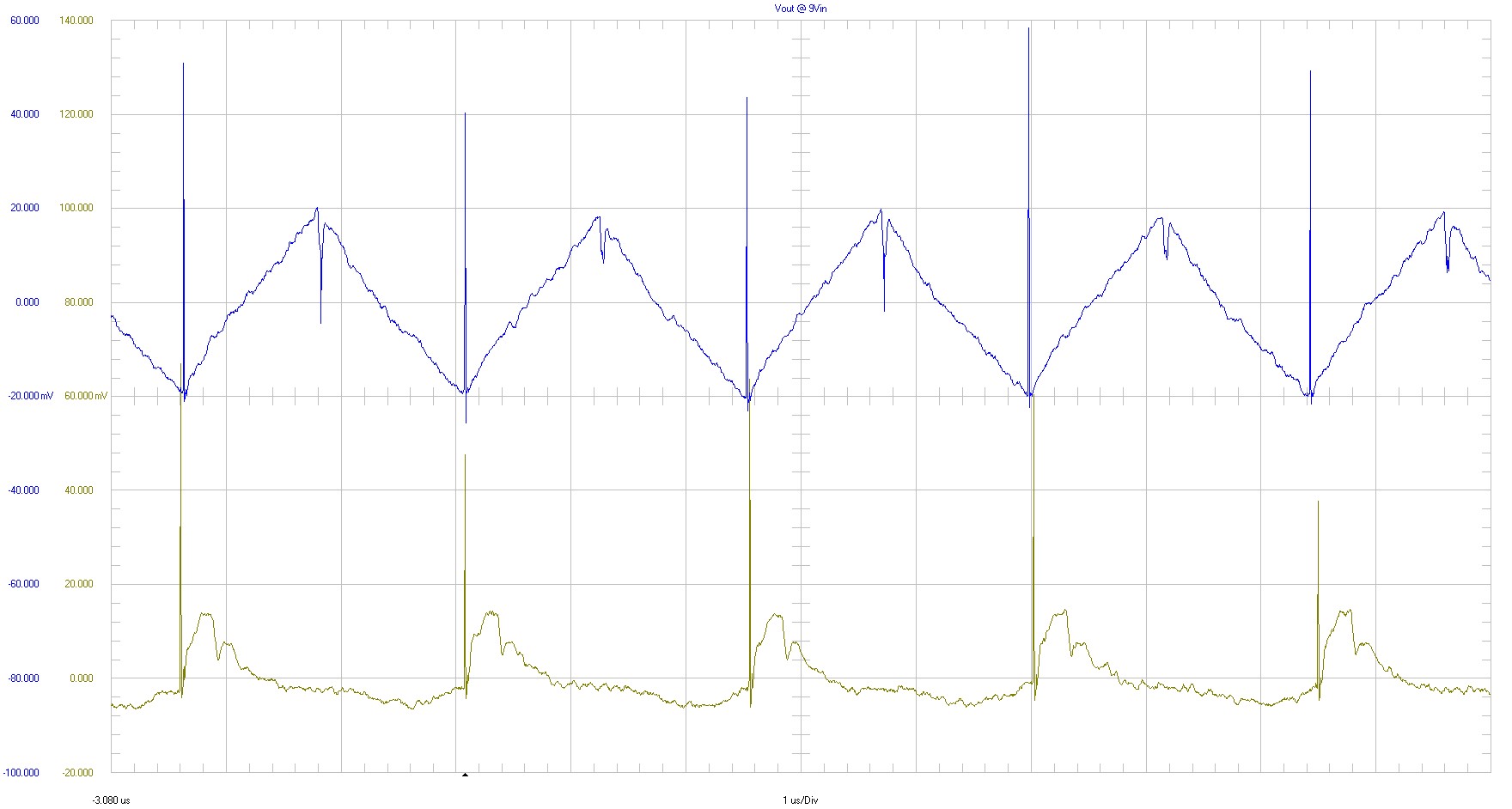
    2. 3.2 Output Voltage Ripple
    3. 3.3 Input Voltage Ripple
    4. 3.4 Load Transients
      1. 3.4.1 9-V Input Voltage
      2. 3.4.2 56-V Input Voltage
    5. 3.5 Start-Up Sequence
      1. 3.5.1 9-V Input Voltage
      2. 3.5.2 56-V Input Voltage
    6. 3.6 Shutdown Sequence
      1. 3.6.1 9-V Input Voltage
      2. 3.6.2 56-V Input Voltage

Output Voltage Ripple

Output voltage ripple is shown in the following figure.

GUID-20220422-SS0I-DC3J-1NKH-W5X2PXNN6MSB-low.jpg

Ch1⇒ VOUT at 9 VIN

20 mV /div


Ch2 ⇒ VOUT at 56 VIN

20 mV /div


AC coupled

20-MHz bandwidth

1 µs/div

Figure 3-9 Output Voltage Ripple