TIDT286 June   2022


  1.   Description
  2.   Features
  3.   Applications
  4. 1Test Prerequisites
    1. 1.1 Voltage and Current Requirements
    2. 1.2 Considerations
    3. 1.3 Dimensions
  5. 2Testing and Results
    1. 2.1 Efficiency Graph
    2. 2.2 Loss Graph
    3. 2.3 Load Regulation
    4. 2.4 Line Regulation
    5. 2.5 Thermal Images
      1. 2.5.1 0.5-A Output Current
      2. 2.5.2 1-A Output Current
      3. 2.5.3 1.5-A Output Current
      4. 2.5.4 2-A Output Current
      5. 2.5.5 Pulsed Ouput Current
    6. 2.6 Bode Plots
      1. 2.6.1 6-V Input Voltage
      2. 2.6.2 12-V Input Voltage
  6. 3Waveforms
    1. 3.1 Switching
      1. 3.1.1 Transistor Q1
        1. 3.1.1.1 Drain - Source
        2. 3.1.1.2 Gate - Source
      2. 3.1.2 Diode D3
    2. 3.2 Input Voltage Ripple
      1. 3.2.1 20-MHz Bandwidth
      2. 3.2.2 Full Bandwidth
    3. 3.3 Output Voltage Ripple
    4. 3.4 Load Transients
      1. 3.4.1 Switching Load From 1 A to 2 A
      2. 3.4.2 Switching Load From 0.2 A to 2 A
        1. 3.4.2.1 50% Duty Cycle
        2. 3.4.2.2 Low Duty Cycle (TON = 3 ms; TOFF = 30 ms)
    5. 3.5 Start-Up Sequence
    6. 3.6 Shutdown Sequence

Start-Up Sequence

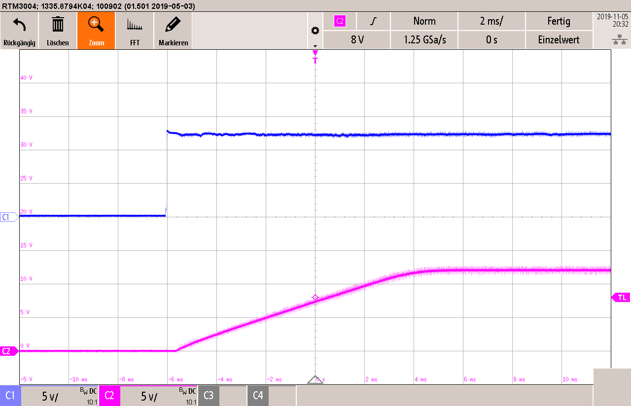
For the waveforms in this section, the electronic load was set to 2 A and the power supply was plugged in.

The soft start takes 10 ms at maximum load.
GUID-20220524-SS0I-X9GQ-GVHQ-JHRZDXCDSBWM-low.png

C1 ⇒ VIN

5 V / div


C2 ⇒ VOUT

5 V / div


2 ms / div

20-MHz bandwidth

Figure 3-13 Start-up With 12-V Input Voltage