TIDT296 September   2022


  1.   Description
  2.   Features
  3.   Applications
  4. 1Test Prerequisites
    1. 1.1 Voltage and Current Requirements
    2. 1.2 Required Equipment
  5. 2Testing and Results
    1. 2.1 Efficiency Graphs
    2. 2.2 Cross Regulation
    3. 2.3 Thermal Images
  6. 3Waveforms
    1. 3.1 Start-Up
    2. 3.2 Undervoltage Protection
    3. 3.3 Output Voltage Ripple
    4. 3.4 Load Transients
    5. 3.5 Switching Node Waveforms
    6. 3.6 Short-Circuit Test
    7. 3.7 Diode Voltage Stress

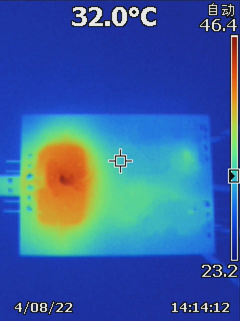
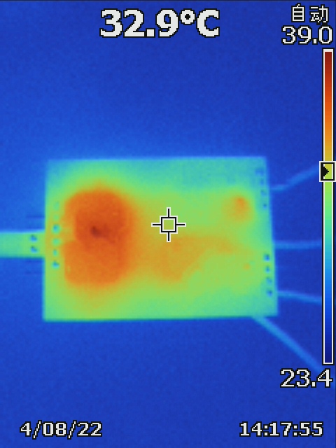
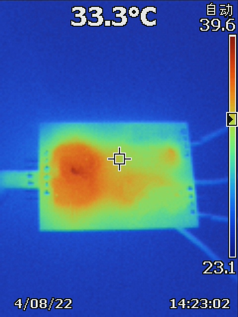
Thermal Images

All thermal images were captured in 25ºC ambient, after a 30-minute warm up.

The following thermal images are at VIN = 10 V, IOUT1 = 80 mA, and IOUT2 = 80 mA.
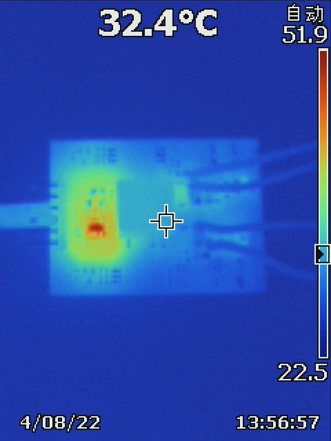
GUID-20220816-SS0I-VPCQ-1XBR-TBL1RWWSRX6L-low.pngFigure 2-4 Top
GUID-20220815-SS0I-V3MT-NZRJ-2LQ1RFW7KGC1-low.pngFigure 2-5 Bottom

The following thermal images are at VIN = 12 V, IOUT1 = 80 mA, and IOUT2 = 80 mA.
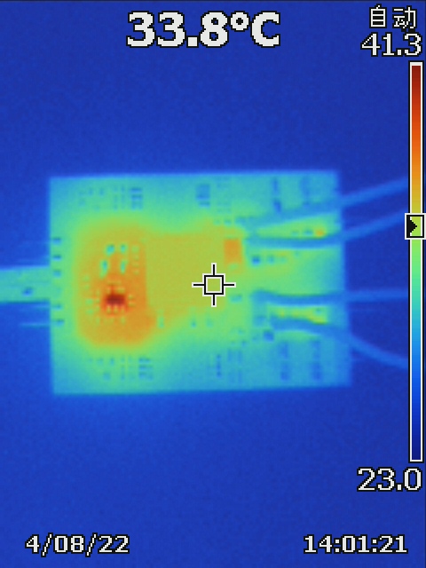
GUID-20220816-SS0I-Q5BL-CDLM-BXNQJR8JV4GD-low.pngFigure 2-6 Top
GUID-20220816-SS0I-FRPS-FNTJ-GDKMMBWKT4J3-low.pngFigure 2-7 Bottom

The following thermal images are at VIN = 20 V, IOUT1 = 80 mA, and IOUT2 = 80 mA.
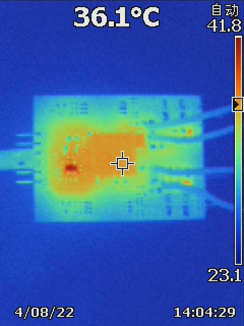
GUID-20220816-SS0I-BRD8-8VWT-93JLFXXS5WCZ-low.pngFigure 2-8 Top
GUID-20220816-SS0I-QVRV-KML1-BNHZ3WDCZSQF-low.pngFigure 2-9 Bottom