Low-Profile 140-W Full-Bridge Reference Design
Description
This power supply is a 140-W, full-bridge reference design for applications requiring high density and low component heights due to the planar transformer. The design is based on a hard-switched full bridge topology, using Schottky diodes on the secondary side, driven by the LM5045. A planar transformer is used to minimize the footprint and height. The printed circuit board (PCB) has six layers and the components are assembled top and bottom. The unit is designed for continuous operation at a rated load at TA < 40°C. A minimum airflow of 200 linear feet per minute (LFM) is recommended for higher ambient temperature.
Features
- Low-profile, 140-W, full-bridge power converter
- 19-VDC to 30-VDC input, 56 VDC 2.5-A output
- 94.4% peak efficiency at 18-VDC input and 56-W load
- Compact board dimensions: 47 mm × 84.2 mm, 11.34-mm height
Applications
 Top Photo
 Bottom Photo
1 Test Prerequisites
1.1 Voltage and Current Requirements
| Parameter | Specifications |
|---|---|
| Input Voltage | 19 VDC to 30 VDC |
| Output Voltage | 56 VDC |
| Output Current | 2.5 A |
1.2 Required Equipment
- 15 VDC to 32 VDC, minimum output current 10 A, constant voltage source (VS1)
- Electronic load, in constant current regulation, range 0 to 3 A (EL1)
- Electric fan 200 LFM
- Oscilloscope (minimum 200-MHz bandwidth)
- Current probe (minimum 100-kHz bandwidth)
- Optional: infrared camera
1.3 Considerations
The board is built on PCB PMP30900RevA.
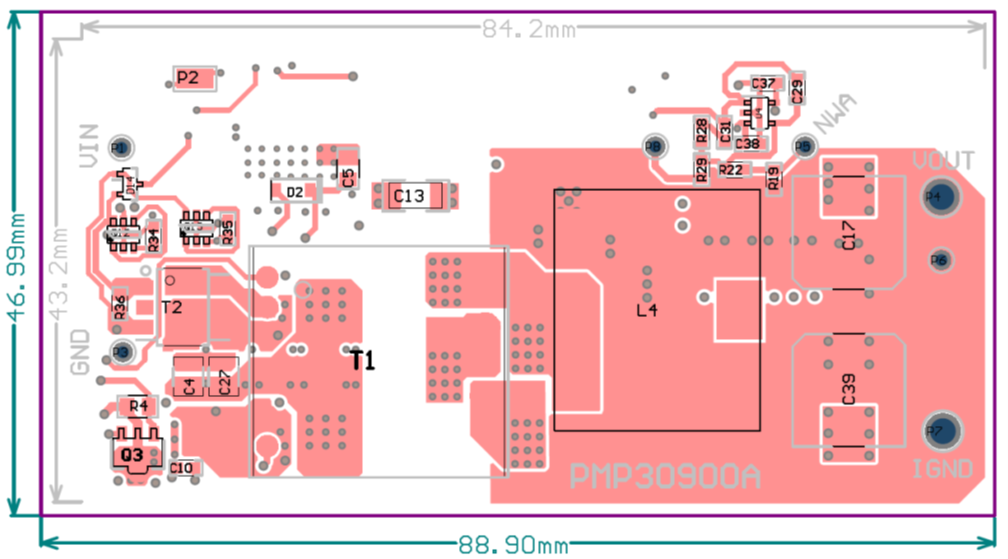
1.4 Dimensions
The board dimensions are 88.9 mm × 46.99 mm, with the height of 11.34 mm (Transformer T1), while the net PCB area dimensions are 84.22 mm x 43.2 mm.
The copper thickness of the six layer board is 70 µm on the outer layers and 35 µm on the inner layers (70-30-30-30-30-70).
1.5 Test Setup
- Connect the source VS1 to P1 (positive) and P3 (negative).
- Add an electrolytic capacitor (> 1 mF, ESR < 30 mΩ) close to input terminals in case long cables from VS1 are used
- Connect the load EL1 to P4 and P7 (P7 is the secondary side ground)
- Attach a current probe in series to EL1 to measure the output current during load transients
- Turn on VS1
- Increase the load current (maximum current 2.5 A)
2 Testing and Results
2.1 Efficiency Graphs
Figure 2-1 shows the efficiency graph of the power supply versus output current. The input voltage has been set to 18 VDC, 24 VDC, and 30 VDC.
 Figure 2-1 Efficiency Graph
2.2 Efficiency Data
Efficiency data is shown in the following tables.
| VIN (V) | IIN (A) | PIN (W) | VOUT (V) | IOUT (A) | POUT (W) | Efficiency (%) |
|---|---|---|---|---|---|---|
| 18.010 | 0.022 | 0.398 | 56.300 | 0.000 | 0 | 0.0% |
| 18.010 | 0.242 | 4.357 | 56.300 | 0.050 | 2.815 | 64.61% |
| 18.000 | 0.406 | 7.306 | 56.300 | 0.101 | 5.703 | 78.06% |
| 18.050 | 0.723 | 13.050 | 56.290 | 0.200 | 11.281 | 86.44% |
| 18.040 | 1.724 | 31.101 | 56.290 | 0.503 | 28.291 | 90.97% |
| 18.018 | 3.327 | 59.946 | 56.210 | 1.007 | 56.603 | 94.42% |
| 18.023 | 6.681 | 120.412 | 56.260 | 2.002 | 112.63 | 93.54% |
| 18.030 | 8.384 | 151.164 | 56.250 | 2.501 | 140.68 | 93.07% |
| VIN (V) | IIN (A) | PIN (W) | VOUT (V) | IOUT (A) | POUT (W) | Efficiency (%) |
|---|---|---|---|---|---|---|
| 24.070 | 0.016 | 0.378 | 56.300 | 0.000 | 0 | 0.0% |
| 24.040 | 0.205 | 4.938 | 56.300 | 0.051 | 2.866 | 58.04% |
| 24.000 | 0.336 | 8.059 | 56.300 | 0.101 | 5.664 | 70.28% |
| 24.000 | 0.567 | 13.603 | 56.290 | 0.200 | 11.264 | 82.80% |
| 24.000 | 1.305 | 31.320 | 56.280 | 0.503 | 28.326 | 90.44% |
| 24.080 | 2.559 | 61.621 | 56.260 | 1.004 | 56.491 | 91.67% |
| 24.070 | 5.084 | 122.372 | 56.250 | 2.016 | 113.40 | 92.67% |
| 24.070 | 6.343 | 152.676 | 56.240 | 2.506 | 140.94 | 92.31% |
| VIN (V) | IIN (A) | PIN (W) | VOUT (V) | IOUT (A) | POUT (W) | Efficiency (%) |
|---|---|---|---|---|---|---|
| 30.03 | 0.0170 | 0.511 | 56.25 | 0 | 0 | 0.0% |
| 30.02 | 0.1817 | 5.455 | 56.26 | 0.0507 | 2.852 | 52.29% |
| 30.02 | 0.3012 | 9.042 | 56.27 | 0.1004 | 5.650 | 62.48% |
| 30.01 | 0.4733 | 14.204 | 56.27 | 0.2014 | 11.333 | 79.79% |
| 30.05 | 1.0913 | 32.794 | 56.27 | 0.5035 | 28.332 | 86.39% |
| 30.04 | 2.096 | 62.964 | 56.26 | 1.004 | 56.479 | 89.70% |
| 30.01 | 4.130 | 123.941 | 56.24 | 2.014 | 113.27 | 91.39% |
| 30.03 | 5.153 | 154.745 | 56.24 | 2.508 | 141.05 | 91.15% |
2.3 Thermal Images
The graphs in Figure 2-2 and Figure 2-3 show the thermal pictures of the converter supplied at 24 VDC at full load. Table 2-4 and Table 2-5 represent the corresponding values of the main image markers.
Thermal shots were taken after the board was running for 30 minutes at an ambient temperature of 25°C.
The board runs at full load with a fan, placed on the right side of the prototype.
2.3.1 Top Side
 Figure 2-2 Thermal Image: Top
View
Figure 2-2 Thermal Image: Top
View| Name | Temperature | Emissivity | Background |
|---|---|---|---|
| T1 | 59.9°C | 0.96 | 25.5°C |
| T1 Core | 55.3°C | 0.96 | 25.5°C |
| Diodes (secondary side) | 56.4°C | 0.96 | 25.5°C |
| L4 | 39.8°C | 0.96 | 25.5°C |
2.3.2 Bottom Side
 Figure 2-3 Thermal Image: Bottom Side
| Name | Temperature | Emissivity | Background |
|---|---|---|---|
| Q9 | 55.9°C | 0.96 | 25.5°C |
| Q7 | 55.5°C | 0.96 | 25.5°C |
| D19 | 69.6°C | 0.96 | 25.5°C |
| D18 | 65.3°C | 0.96 | 25.5°C |
| R11 | 66.5°C | 0.96 | 25.5°C |
| R17 | 68.5°C | 0.96 | 25.5°C |
| Q1 | 46.3°C | 0.96 | 25.5°C |
| D15 | 66.0°C | 0.96 | 25.5°C |
| U1 | 44.6°C | 0.96 | 25.5°C |
| Q8 | 52.2°C | 0.96 | 25.5°C |
| Q6 | 54.5°C | 0.96 | 25.5°C |
2.4 Bode Plots
The graph in Figure 2-4 shows the bode plot of the converter, when supplied at 24 VDC and loaded at 2.5 A. Here are the results, in terms of crossover frequency, phase margin, and gain margin:
| Parameter | Full Load |
|---|---|
| Crossover frequency | 2.859 kHz |
| Phase margin | 80.84° |
| Gain margin | 29.25 dB |
 Figure 2-4 Bode Plot
3 Waveforms
3.1 Switching
The switching waveforms were measured by supplying the converter at 30 VDC and full load.
3.1.1 Secondary Side
The waveform in Figure 3-1 represents the switching behavior measured on diode D4-cathode to IGND.
)") Figure 3-1 Switch-Node Secondary Side (50
V / div, 500 ns / div, no bandwidth limit (BWL))
Figure 3-1 Switch-Node Secondary Side (50
V / div, 500 ns / div, no bandwidth limit (BWL))3.1.2 Primary Side
3.1.2.1 Transistor Q8 Drain-Source
") Figure 3-2 Switch-Node Q8 Drain to Source
(10 V / div, 1 µs / div, no BWL)
Figure 3-2 Switch-Node Q8 Drain to Source
(10 V / div, 1 µs / div, no BWL)3.1.2.2 HS2-Pin of U1
3.1.2.2.1 Undershoot
 of U1
(10 V / div, 80 ns / div, no BWL), Detail of Undershoot") Figure 3-3 Voltage on HS2 pin (16) of U1
(10 V / div, 80 ns / div, no BWL), Detail of Undershoot
Figure 3-3 Voltage on HS2 pin (16) of U1
(10 V / div, 80 ns / div, no BWL), Detail of Undershoot 3.1.2.2.2 Overshoot
, Detail of
Overshoot") Figure 3-4 Voltage on HS2 pin 16 of U1 (10 V / div, 10 ns / div, no BWL), Detail of
Overshoot
Figure 3-4 Voltage on HS2 pin 16 of U1 (10 V / div, 10 ns / div, no BWL), Detail of
Overshoot 3.2 Output Voltage Ripple
The output voltage ripple was measured by supplying the converter at 24 VDC and full load; the bandwidth limit of the scope was set to 20 MHz.
, AC Coupling, 20-MHz BWL)") Figure 3-5 Output Voltage
(10 mV/ div, 2 µs /div), AC Coupling, 20-MHz BWL)
Figure 3-5 Output Voltage
(10 mV/ div, 2 µs /div), AC Coupling, 20-MHz BWL)3.3 Load Transients
The output voltage variation, during load transients, was measured by supplying the converter at 24 VDC and by switching the load current between 1.25 A and 2 A. For all waveforms, the bandwidth limit of the oscilloscope was set to 20 MHz
 Figure 3-6 Load Transients 1.25 A to 2 A
- Channel C4: Output voltage (500 mV / div, 2 ms / div, AC coupling)
- Channel C3: Output current (1 A / div, DC coupling)
3.4 Start-Up Sequence
The screen shots in Figure 3-7 and Figure 3-8 show the output voltage behavior during start-up, at VIN = 24 VDC.
3.4.1 Full Load
 Figure 3-7 Start-Up With Full
Load
Figure 3-7 Start-Up With Full
Load- Channel C2: Input voltage (5 V /div, 10 ms / div, DC coupling, 20-MHz BWL)
- Channel C4: Output voltage (20 V/div, DC coupling, 20-MHz BWL)
3.4.2 Zero Load
 Figure 3-8 Start-Up With Zero
Load
Figure 3-8 Start-Up With Zero
Load- Channel C2: Input voltage (5 V/ div, 10 ms / div, DC coupling, 20-MHz BWL)
- Channel C4: Output voltage (20 V/ div, DC coupling, 20-MHz BWL)
3.4.3 Overload
The following screen shots (Figure 3-9 and Figure 3-10) show the output voltage during start-up and overload protection, when the converter was loaded at 3.5 A.
, Time Base: 10 ms / div") Figure 3-9 Start-Up With Overload Condition (3.5 A), Time Base: 10 ms / div
Figure 3-9 Start-Up With Overload Condition (3.5 A), Time Base: 10 ms / div- Channel C4: Output voltage (10 V /div, 10 ms / div, DC coupling, 20-MHz BWL)
The same condition as in Figure 3-9 with different time base results in Figure 3-10.
, Time Base: 100 ms / div") Figure 3-10 Start-Up With Overload Condition (3.5 A), Time Base: 100 ms / div
Figure 3-10 Start-Up With Overload Condition (3.5 A), Time Base: 100 ms / div- Channel C4: Output voltage (10 V / div, 100 ms / div, DC coupling, 20-MHz BWL)
3.5 Shutdown Sequence
The output voltage has been measured by switching off the DC voltage source while the load was set to 2.5 A and VIN to 24 VDC
 Figure 3-11 Shutdown Sequence
- Channel C2: Input voltage (5 V/ div, 10 ms /div, DC coupling, 20-MHz BWL)
- Channel C4: Output voltage (20 V / div, DC coupling, 20-MHz BWL)
IMPORTANT NOTICE AND DISCLAIMER
TI PROVIDES TECHNICAL AND RELIABILITY DATA (INCLUDING DATASHEETS), DESIGN RESOURCES (INCLUDING REFERENCE DESIGNS), APPLICATION OR OTHER DESIGN ADVICE, WEB TOOLS, SAFETY INFORMATION, AND OTHER RESOURCES “AS IS” AND WITH ALL FAULTS, AND DISCLAIMS ALL WARRANTIES, EXPRESS AND IMPLIED, INCLUDING WITHOUT LIMITATION ANY IMPLIED WARRANTIES OF MERCHANTABILITY, FITNESS FOR A PARTICULAR PURPOSE OR NON-INFRINGEMENT OF THIRD PARTY INTELLECTUAL PROPERTY RIGHTS.
These resources are intended for skilled developers designing with TI products. You are solely responsible for (1) selecting the appropriate TI products for your application, (2) designing, validating and testing your application, and (3) ensuring your application meets applicable standards, and any other safety, security, or other requirements. These resources are subject to change without notice. TI grants you permission to use these resources only for development of an application that uses the TI products described in the resource. Other reproduction and display of these resources is prohibited. No license is granted to any other TI intellectual property right or to any third party intellectual property right. TI disclaims responsibility for, and you will fully indemnify TI and its representatives against, any claims, damages, costs, losses, and liabilities arising out of your use of these resources.
TI’s products are provided subject to TI’s Terms of Sale (www.ti.com/legal/termsofsale.html) or other applicable terms available either on ti.com or provided in conjunction with such TI products. TI’s provision of these resources does not expand or otherwise alter TI’s applicable warranties or warranty disclaimers for TI products.
Mailing Address: Texas Instruments, Post Office Box 655303, Dallas, Texas 75265
Copyright © 2022, Texas Instruments Incorporated