TIDT327 may 2023
2.3 Thermal Images
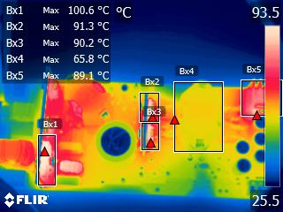
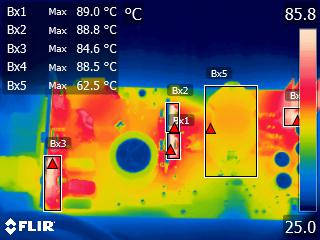
Thermal images are shown in the following figures. All figures were taken after a 30 minute soak in a container with no external fan.

90 VAC full load, Bx1 = Diode
bridge; Bx2 = Qclamp;
Bx3 = Qpri; Bx4 = XFMR; Bx5 = SR FET
Figure 2-3 Thermal ImageBx3 = Qpri; Bx4 = XFMR; Bx5 = SR FET

120 VAC full load, Bx3 = Diode
bridge;
Bx2 = Qclamp; Bx1 = Qpri; Bx5 = XFMR; Bx4 = SR FET
Figure 2-4 Thermal ImageBx2 = Qclamp; Bx1 = Qpri; Bx5 = XFMR; Bx4 = SR FET