TIDT327 may 2023
3.1 Switching
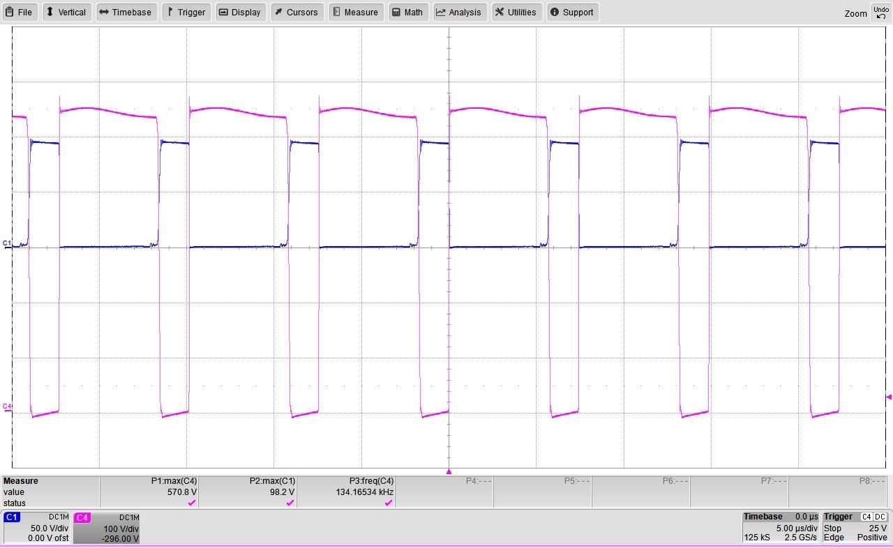
The primary and secondary switch nodes of the ACF are shown in the following images at various loads.
Figure 3-22 has the following parameters:
- Ch4 (Magenta): Q2 Switch node voltage (100 V/div), full bandwidth
- Ch1 (Blue): Q17 SR Switch node voltage (50 V/div), full bandwidth
- Timebase: 5 μs/div.
 Figure 3-1 265 VAC; 22 V at 9.5 A;
ƒSW = 134 kHz; Maximum Stress on: Q1 = 570.8 V; Q17 = 98.2
V
Figure 3-1 265 VAC; 22 V at 9.5 A;
ƒSW = 134 kHz; Maximum Stress on: Q1 = 570.8 V; Q17 = 98.2
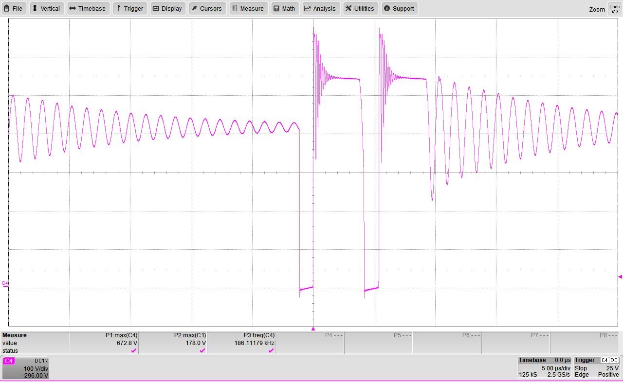
VFigure 3-2 has the following parameters:
- Ch4 (Magenta): Q2 Switch node voltage (100 V/div), full bandwidth
- Timebase: 5 μs/div
 Figure 3-2 265 VAC; 22 V at 2 A; (LPM to
ABM); Maximum Stress on: Q1 = 672 V
Figure 3-2 265 VAC; 22 V at 2 A; (LPM to
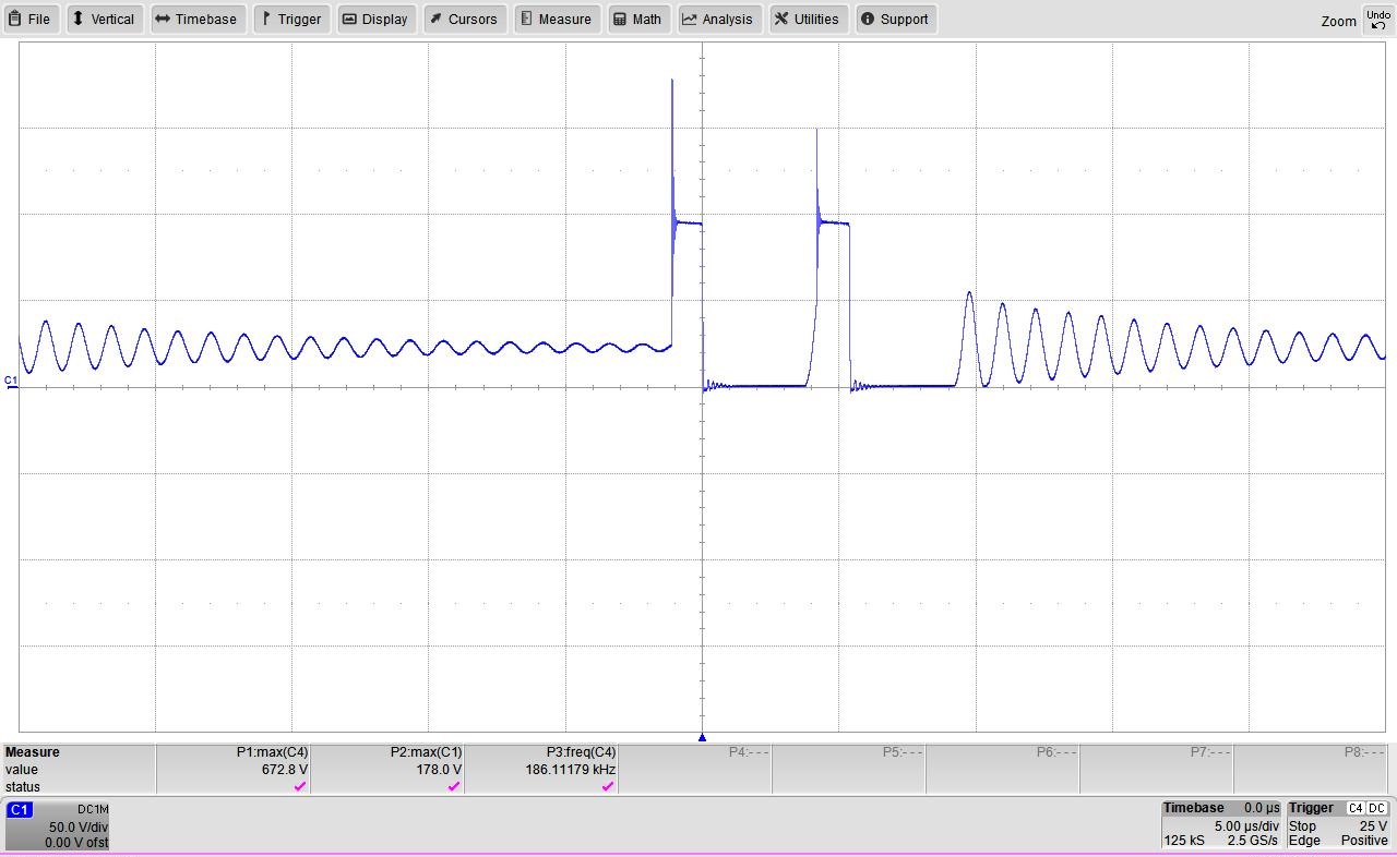
ABM); Maximum Stress on: Q1 = 672 VFigure 3-3 has the following parameters:
- Ch1(blue): SR Switch node voltage (50 V/div) full bandwidth
- Timebase: 5 μs/div
 Figure 3-3 265 VAC; 22 V at 2 A; (LPM to
ABM); Maximum Stress on: Q17 = 178 V