TIDT328 april   2023


  1.   1
  2.   Description
  3.   Features
  4.   Applications
  5. 1Test Prerequisites
    1. 1.1 Voltage and Current Requirements
    2. 1.2 Considerations
    3. 1.3 Dimensions
  6. 2Testing and Results
    1. 2.1 Efficiency Graphs
    2. 2.2 Load Regulation
    3. 2.3 Thermal Images
      1. 2.3.1 Unmodulated 60 VDC - Output
      2. 2.3.2 60 VAC - Output Modulated With 120-Hz Sinus (0 V – 5 V)
      3. 2.3.3 Conclusion
    4. 2.4 Bode Plot at Maximum Duty Cycle
  7. 3Waveforms
    1. 3.1 Switching
      1. 3.1.1 Transistor Q1 Operating in Deep DCM
        1. 3.1.1.1 Drain to Source
        2. 3.1.1.2 Gate to Source
      2. 3.1.2 Diode D3 (Referenced to VOUT)
    2. 3.2 Output Voltage Ripple
    3. 3.3 Input Voltage Ripple
    4. 3.4 Start-Up Sequence
    5. 3.5 Shutdown Sequence
  8.   A Modulating the Output Voltage
    1.     A.1 Revision B
      1.      A.1.1 Bode Plot
      2.      A.1.2 Simulation
      3.      A.1.3 Measured Waveforms
        1.       A.1.3.1 Sinus 40 Hz
        2.       A.1.3.2 Sinus 100 Hz
        3.       A.1.3.3 Sawtooth 1
        4.       A.1.3.4 Sawtooth 2
        5.       A.1.3.5 Pure Triangle
        6.       A.1.3.6 Conclusion
    2.     A.2 Revision C
      1.      A.2.1 Bode Plot
      2.      A.2.2 Measured Waveforms
        1.       A.2.2.1 Sinus 120 Hz
        2.       A.2.2.2 Sawtooth 1
        3.       A.2.2.3 Sawtooth 2
        4.       A.2.2.4 Pure Triangle
      3.      A.2.3 Analysis Capacitor 1 µF, 100 V, X7R, 1206
        1.       A.2.3.1 DC-Bias
        2.       A.2.3.2 Resistance (ESR)
        3.       A.2.3.3 Reactance
        4.       A.2.3.4 Impedance

Bode Plot

Three output capacitors (2.2 µF, 100 V, 1210, X7R) are assembled in revision B of this reference design.
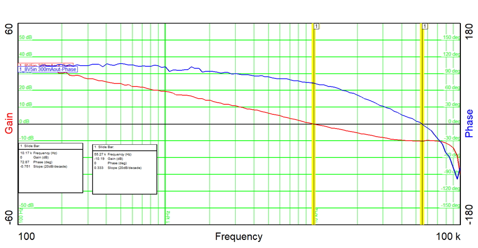
GUID-20230314-SS0I-ZWB8-ZSWK-RP6TTVRMHBQR-low.jpg Figure 4-1 Bode Plot, Revision B, Worst Case is 8.5 VIN, 0.3 AOUT

The plot in Figure 4-1 shows the worst-case Bode plot for output capacitance, 3 × 2.2 µF and fCO 10 kHz (R13 4.02 kΩ, C16 100 nF, C15 390 pF); despite achieved crossover frequency, fCO, 10 kHz the modulated sinusoidal waveform showed non linearity beyond fmod 40 Hz+, similar to the simulation seen in Figure 4-2: the output voltage drops, discharge current of output capacitor drops, the sinusoidal function converts into an e-function.