TIDT349 January 2024
- 1
- Description
- Features
- Applications
- 1Test Prerequisites
- 2Testing and Results
-
3Waveforms
- 3.1 Charge Mode Start-Up Waveform
- 3.2 OTG Mode Start-Up Waveform
- 3.3 Voltage Transition at OTG Mode
- 3.4 Ripple and Noise at OTG Mode
- 3.5 Load Transients at OTG Mode
- 3.6 Switching Waveform
- 3.7 Overcurrent Protection at OTG Mode
- 3.8 Short-Circuit Protection at OTG Mode
- 3.9 Short-Circuit Protection at Charge Mode
2.3 Thermal Images
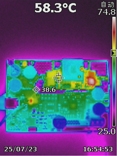
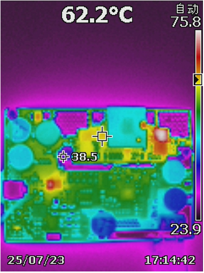
Table 2-4 shows the thermal images at full power charge mode and OTG mode. All images were captured at 25ºC ambient temperature, after a 30-minute warm up.
Table 2-4 Thermal Results: Full Power
Charge Mode and OTG Mode
| Temperature(°C) | Test Condition | |
|---|---|---|
| Component | Charge Mode (20Vsys to 10S BAT Full Load) | OTG Mode (42V BAT to 20V at 5A, 100W) |
| Q2 (Vsys high side) | 59.4 | 63.1 |
| Q4 (Vsys low side) | 58.6 | 60.2 |
| Q1(Vbat high side) | 64 | 76.8 |
| Q3 (Vbat low side) | 73.6 | 66.8 |
| Buck-Boost inductor | 64.2 | 66.3 |
| TPS25751 | 68.6 | 72.2 |
| BQ25756 | 53.2 | 57.3 |
| Rsense (Input) | 61.5 | 62.1 |
| Rsense (CHG) | 52.6 | 53.2 |
 Figure 2-5 Charge Mode From 20Vsys to
42V Vbat Full Load
 Figure 2-6 OTG Mode From Vbat = 42V
to 20V at 5A