TIDT349A January 2024 – December 2024
- 1
- Description
- Features
- Applications
- 1Test Prerequisites
- 2Testing and Results
-
3Waveforms
- 3.1 Charge Mode Start-Up Waveform
- 3.2 OTG Mode Start-Up Waveform
- 3.3 Voltage Transition at OTG Mode
- 3.4 Ripple and Noise at OTG Mode
- 3.5 Load Transients at OTG Mode
- 3.6 Switching Waveform
- 3.7 Overcurrent Protection at OTG Mode
- 3.8 Short-Circuit Protection at OTG Mode
- 3.9 Short-Circuit Protection at Charge Mode
- 4Trademarks
2.1 Efficiency Graphs
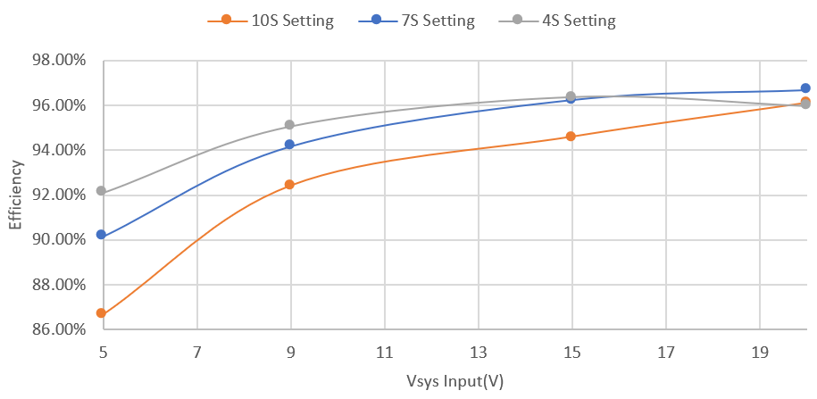
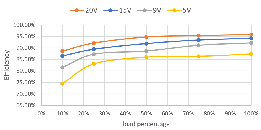
Figure 2-1 shows the sink mode efficiency across different Vsys voltage and battery cell conditions. The fast charge current limit is set to 3A and input current limit is set to 3A for 5V, 9V, and 15V input source, and 5A for a 20V input source. At OTG mode, Figure 2-3 shows the efficiency test which was performed at the 10S battery setting.
 Figure 2-1 Charge Mode Efficiency Across Vsys and Vbat
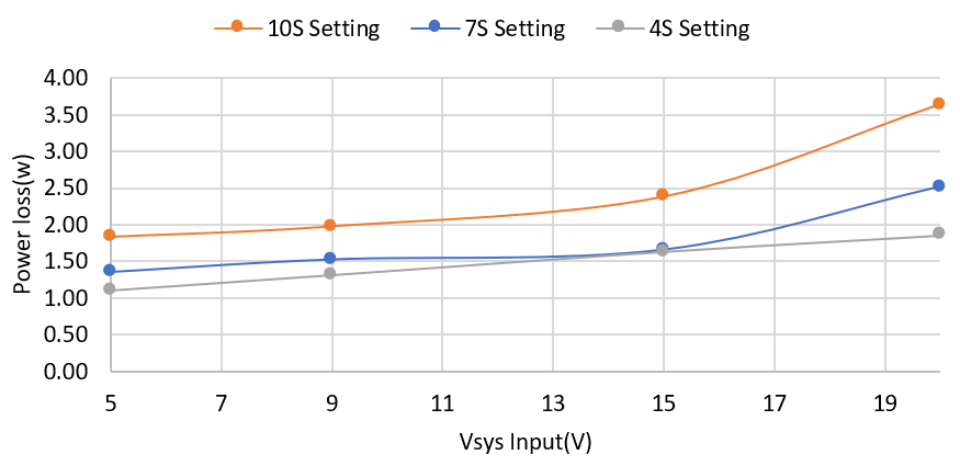
 Figure 2-2 Power Loss vs Vsys and Vbat
 Figure 2-3 OTG Mode 20V at 5A Full-Load Efficiency Vbat = 40V
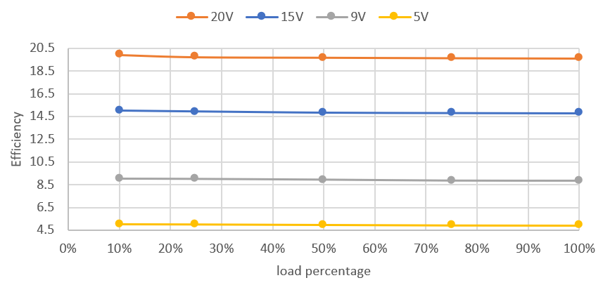
 Figure 2-4 OTG Mode Output Voltage Regulation vs Load