TIDT382 February   2024


  1.   1
  2.   Description
  3.   Features
  4.   Applications
  5. 1Test Prerequisites
    1. 1.1 Voltage and Current Requirements
    2. 1.2 Considerations
    3. 1.3 Dimensions
  6. 2Testing and Results
    1. 2.1 Efficiency Graphs
      1. 2.1.1 LM25180-Q1 Efficiency Graph
      2. 2.1.2 SN6507-Q1 Efficiency Graph
      3. 2.1.3 UCC14130-Q1 Efficiency Graph
      4. 2.1.4 UCC25800-Q1 Efficiency Graph
      5. 2.1.5 Efficiency Comparison
    2. 2.2 Efficiency Data
      1. 2.2.1 LM25180-Q1 Efficiency Data
      2. 2.2.2 SN6507-Q1 Efficiency Data
      3. 2.2.3 UCC14130-Q1 Efficiency Data
      4. 2.2.4 UCC25800-Q1 Efficiency Data
    3. 2.3 Load Regulation
      1. 2.3.1 LM25180-Q1 Load Regulation
      2. 2.3.2 SN6507-Q1 Load Regulation
      3. 2.3.3 UCC14130-Q1 Load Regulation
      4. 2.3.4 UCC25800-Q1 Load Regulation
      5. 2.3.5 Load Regulation Comparison
    4. 2.4 Thermal Images
      1. 2.4.1 LM25180-Q1 Thermal Image
      2. 2.4.2 SN6507-Q1 Thermal Image
      3. 2.4.3 UCC14130-Q1 Thermal Image
      4. 2.4.4 UCC25800-Q1 Thermal Image
    5. 2.5 Common-Mode Current (CMI)
      1. 2.5.1 LM25180-Q1 CMI
      2. 2.5.2 SN6507-Q1 CMI
      3. 2.5.3 UCC14130-Q1 CMI
      4. 2.5.4 UCC25800-Q1 CMI
      5. 2.5.5 Common-Mode Current Comparison
  7. 3Waveforms
    1. 3.1 Switching
      1. 3.1.1 LM25180-Q1 Switching
      2. 3.1.2 SN6507-Q1 Switching
      3. 3.1.3 UCC25800-Q1 Switching
    2. 3.2 Output Voltage Ripple
      1. 3.2.1 LM25180-Q1 Output Voltage Ripple
      2. 3.2.2 SN6507-Q1 Output Voltage Ripple
      3. 3.2.3 UCC14130-Q1 Output Voltage Ripple
      4. 3.2.4 UCC25800-Q1 Output Voltage Ripple
      5. 3.2.5 Output Voltage Ripple Comparison
    3. 3.3 Input Voltage Ripple
      1. 3.3.1 LM25180-Q1 Input Voltage Ripple
      2. 3.3.2 SN6507-Q1 Input Voltage Ripple
      3. 3.3.3 UCC14130-Q1 Input Voltage Ripple
      4. 3.3.4 UCC25800-Q1 Input Voltage Ripple
      5. 3.3.5 Input Voltage Ripple Comparison
    4. 3.4 Load Transients
      1. 3.4.1 LM25180-Q1 Load Transients
      2. 3.4.2 SN6507-Q1 Load Transients
      3. 3.4.3 UCC14130-Q1 Load Transients
      4. 3.4.4 UCC25800-Q1 Load Transients
    5. 3.5 Start-Up Sequence
      1. 3.5.1 LM25180-Q1 Start-Up Sequence
      2. 3.5.2 SN6507 Q1 Start Up Sequence
      3. 3.5.3 UCC14130-Q1 Start-Up Sequence
      4. 3.5.4 UCC25800-Q1 Start-Up Sequence
    6. 3.6 Shutdown Sequence
      1. 3.6.1 LM25180-Q1 Shutdown Sequence
      2. 3.6.2 SN6507-Q1 Shutdown Sequence
      3. 3.6.3 UCC14130-Q1 Shutdown Sequence
      4. 3.6.4 UCC25800-Q1 Shutdown Sequence
    7. 3.7 Undervoltage Protection
      1. 3.7.1 LM25180-Q1 Undervoltage Protection
      2. 3.7.2 SN6507-Q1 Undervoltage Protection
      3. 3.7.3 UCC14130-Q1 Undervoltage Protection
      4. 3.7.4 UCC25800-Q1 Undervoltage Protection
  8. 4Summary
  9. 5References

Common-Mode Current Comparison

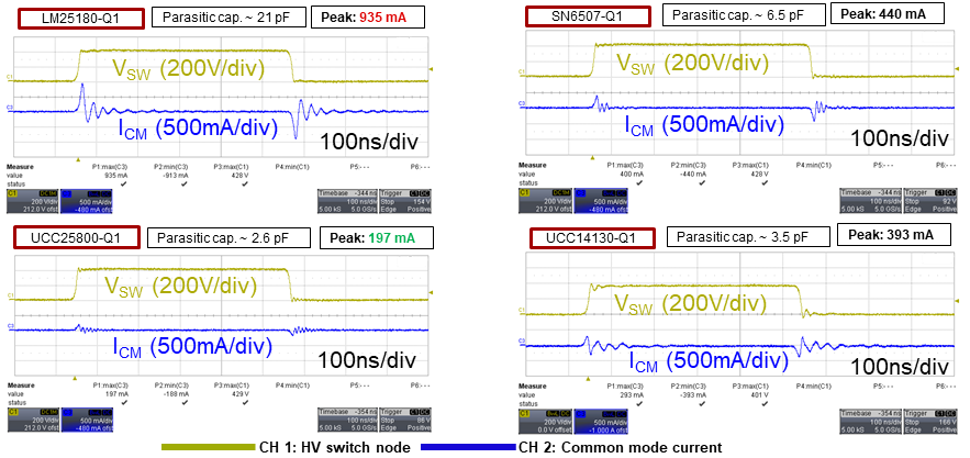
The CMI comparison waveforms of the four topologies are illustrated in the following images.
GUID-20240116-SS0I-XC81-V3J3-S58SXHXPMH9B-low.png
Channel 1: HV switch node, [scale: 200V/div, 100ns/div]
Channel 3: CMI current, [scale: 500mA/div, 100ns/div]
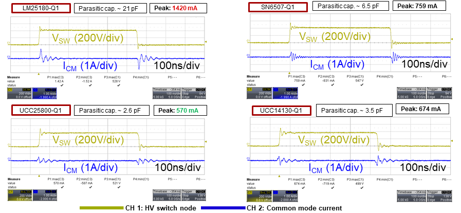
Figure 2-24 Common-Mode Current Comparison at 40V/ns Slew Rate
GUID-20240116-SS0I-5RGW-76QL-BXBKLLN4X9LC-low.png
Channel 1: HV switch node, [scale: 200V/div, 100ns/div]
Channel 3: CMI current, [scale: 1A/div, 100ns/div]
Figure 2-25 Common-Mode Current Comparison at 100V/ns Slew Rate