TIDT382 February   2024


  1.   1
  2.   Description
  3.   Features
  4.   Applications
  5. 1Test Prerequisites
    1. 1.1 Voltage and Current Requirements
    2. 1.2 Considerations
    3. 1.3 Dimensions
  6. 2Testing and Results
    1. 2.1 Efficiency Graphs
      1. 2.1.1 LM25180-Q1 Efficiency Graph
      2. 2.1.2 SN6507-Q1 Efficiency Graph
      3. 2.1.3 UCC14130-Q1 Efficiency Graph
      4. 2.1.4 UCC25800-Q1 Efficiency Graph
      5. 2.1.5 Efficiency Comparison
    2. 2.2 Efficiency Data
      1. 2.2.1 LM25180-Q1 Efficiency Data
      2. 2.2.2 SN6507-Q1 Efficiency Data
      3. 2.2.3 UCC14130-Q1 Efficiency Data
      4. 2.2.4 UCC25800-Q1 Efficiency Data
    3. 2.3 Load Regulation
      1. 2.3.1 LM25180-Q1 Load Regulation
      2. 2.3.2 SN6507-Q1 Load Regulation
      3. 2.3.3 UCC14130-Q1 Load Regulation
      4. 2.3.4 UCC25800-Q1 Load Regulation
      5. 2.3.5 Load Regulation Comparison
    4. 2.4 Thermal Images
      1. 2.4.1 LM25180-Q1 Thermal Image
      2. 2.4.2 SN6507-Q1 Thermal Image
      3. 2.4.3 UCC14130-Q1 Thermal Image
      4. 2.4.4 UCC25800-Q1 Thermal Image
    5. 2.5 Common-Mode Current (CMI)
      1. 2.5.1 LM25180-Q1 CMI
      2. 2.5.2 SN6507-Q1 CMI
      3. 2.5.3 UCC14130-Q1 CMI
      4. 2.5.4 UCC25800-Q1 CMI
      5. 2.5.5 Common-Mode Current Comparison
  7. 3Waveforms
    1. 3.1 Switching
      1. 3.1.1 LM25180-Q1 Switching
      2. 3.1.2 SN6507-Q1 Switching
      3. 3.1.3 UCC25800-Q1 Switching
    2. 3.2 Output Voltage Ripple
      1. 3.2.1 LM25180-Q1 Output Voltage Ripple
      2. 3.2.2 SN6507-Q1 Output Voltage Ripple
      3. 3.2.3 UCC14130-Q1 Output Voltage Ripple
      4. 3.2.4 UCC25800-Q1 Output Voltage Ripple
      5. 3.2.5 Output Voltage Ripple Comparison
    3. 3.3 Input Voltage Ripple
      1. 3.3.1 LM25180-Q1 Input Voltage Ripple
      2. 3.3.2 SN6507-Q1 Input Voltage Ripple
      3. 3.3.3 UCC14130-Q1 Input Voltage Ripple
      4. 3.3.4 UCC25800-Q1 Input Voltage Ripple
      5. 3.3.5 Input Voltage Ripple Comparison
    4. 3.4 Load Transients
      1. 3.4.1 LM25180-Q1 Load Transients
      2. 3.4.2 SN6507-Q1 Load Transients
      3. 3.4.3 UCC14130-Q1 Load Transients
      4. 3.4.4 UCC25800-Q1 Load Transients
    5. 3.5 Start-Up Sequence
      1. 3.5.1 LM25180-Q1 Start-Up Sequence
      2. 3.5.2 SN6507 Q1 Start Up Sequence
      3. 3.5.3 UCC14130-Q1 Start-Up Sequence
      4. 3.5.4 UCC25800-Q1 Start-Up Sequence
    6. 3.6 Shutdown Sequence
      1. 3.6.1 LM25180-Q1 Shutdown Sequence
      2. 3.6.2 SN6507-Q1 Shutdown Sequence
      3. 3.6.3 UCC14130-Q1 Shutdown Sequence
      4. 3.6.4 UCC25800-Q1 Shutdown Sequence
    7. 3.7 Undervoltage Protection
      1. 3.7.1 LM25180-Q1 Undervoltage Protection
      2. 3.7.2 SN6507-Q1 Undervoltage Protection
      3. 3.7.3 UCC14130-Q1 Undervoltage Protection
      4. 3.7.4 UCC25800-Q1 Undervoltage Protection
  8. 4Summary
  9. 5References

LM25180-Q1 Undervoltage Protection

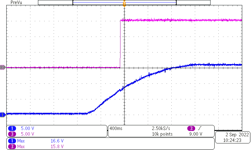
LM25180-Q1 undervoltage protection waveforms are shown in the following figures.
GUID-20240116-SS0I-PM8T-RVWZ-D0CMFQDTN1FC-low.png
Channel 1: Input voltage at start-up with UVLO protection at full Load, [scale: 5V/div, 400ms/div]
Channel 3: Output voltage at start-up with UVLO protection at full Load, [scale: 5V/div, 400ms/div]
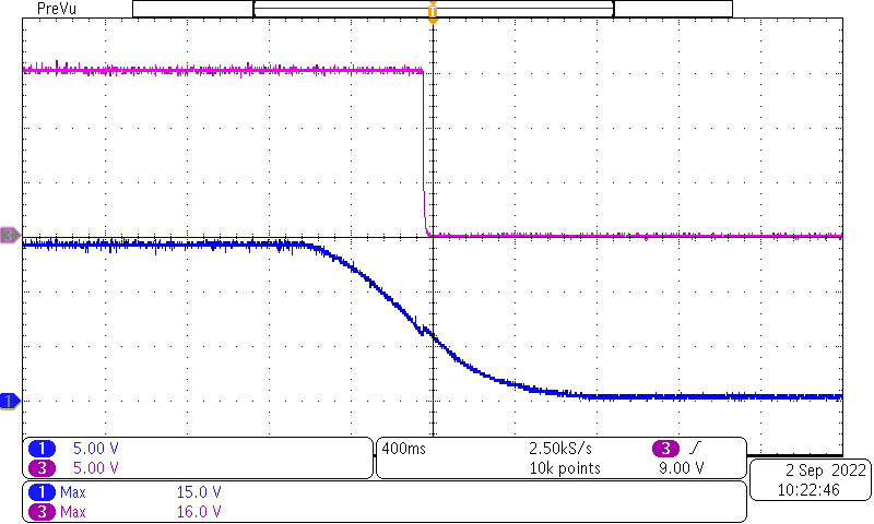
Figure 3-26 LM25180-Q1 UVLO Protection at Rising Input Voltage
GUID-20240116-SS0I-DD7V-KSG1-48F2LJFQZXB1-low.png
Channel 1: Input voltage at shutoff with UVLO protection at full Load, [scale: 5V/div, 400ms/div]
Channel 3: Output voltage at shutoff with UVLO protection at full Load, [scale: 5V/div, 400ms/div]
Figure 3-27 LM25180-Q1 UVLO Protection at Falling Input Voltage