TIDT388 February 2024
3.6 Efficiency and Power Loss Comparison of Varying Solutions
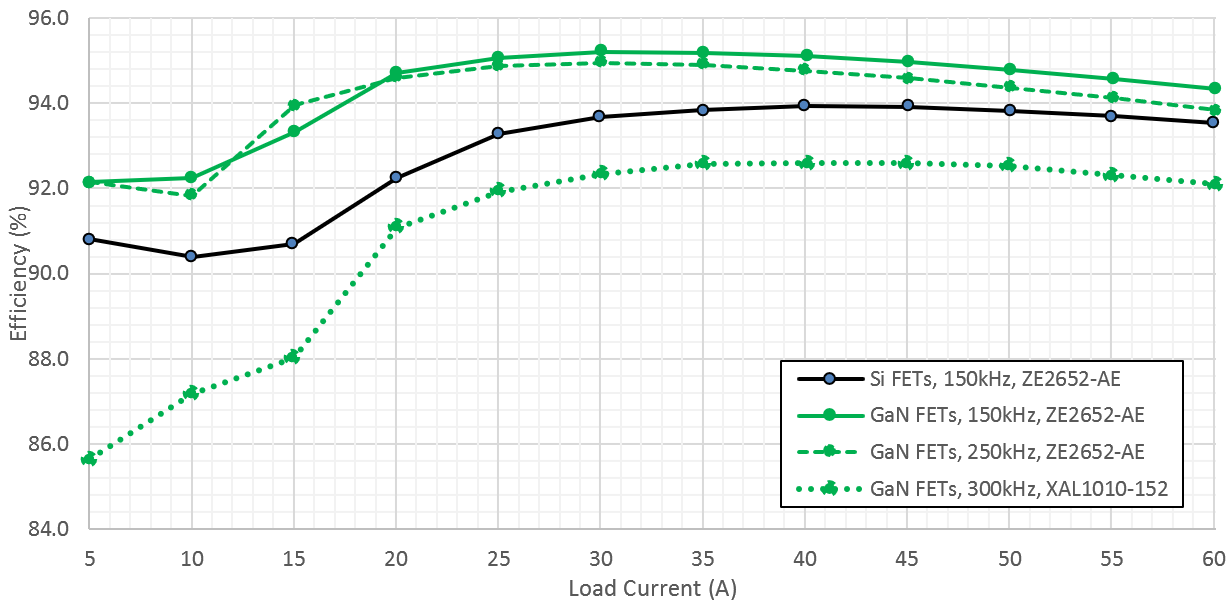
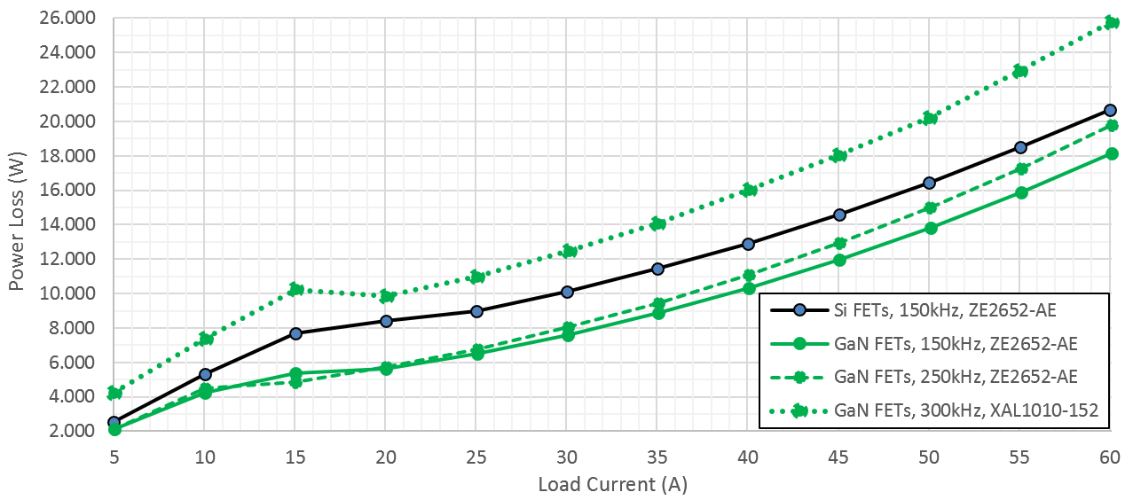
Figure 3-29 and Figure 3-30 show the difference in efficiency and power loss between Silicon FET and GaN FET designs operating at various switching frequencies. Results shown are taken at 48V input voltage.
The PMP23392 design uses LMG3100R017 GaN FETs switching at 300kHz / phase and XAL1010-152 inductors, exemplifying a small solution size. A variant of the PMP23392 design (using LMG3100R017 GaN FETs) except using ZE2652-AE inductors and switching at 150kHz / phase, exemplifies a high-efficiency solution.
PMP23420, a design equivalent to PMP23392, yet using Silicon FETs, ZE2652-AE inductors, and switching at 150kHz / phase, exemplifies a low-cost solution.

Figure 3-29 Efficiency Comparison Between Silicon and GaN FET Solutions at Varying Switching Frequencies (5A to 60A Load)

Figure 3-30 Power Loss Comparison Between Silicon and GaN FET Solutions at Varying Switching Frequencies (5A to 60A Load)