TIDT394 May   2024


  1.   1
  2.   Description
  3.   Features
  4.   Applications
  5. 1Test Prerequisites
    1. 1.1 Voltage and Current Requirements
    2. 1.2 Required Equipment
    3. 1.3 Considerations
    4. 1.4 Dimensions
  6. 2Testing and Results
    1. 2.1 Efficiency Graphs
    2. 2.2 Efficiency Data
    3. 2.3 Thermal Images
    4. 2.4 Bode Plots
  7. 3Waveforms
    1. 3.1 Switching
    2. 3.2 Voltage Ripple
    3. 3.3 Short-Circuit Protection
    4. 3.4 Load Transients
    5. 3.5 Start-up Sequence
    6. 3.6 Current Monitor Output

Start-up Sequence

Figure 3-7 and Figure 3-8 show start-up behavior for PMP23389. The power supply was enabled using the ENABLE signal or by shorting TP8 to TP9 on the board.
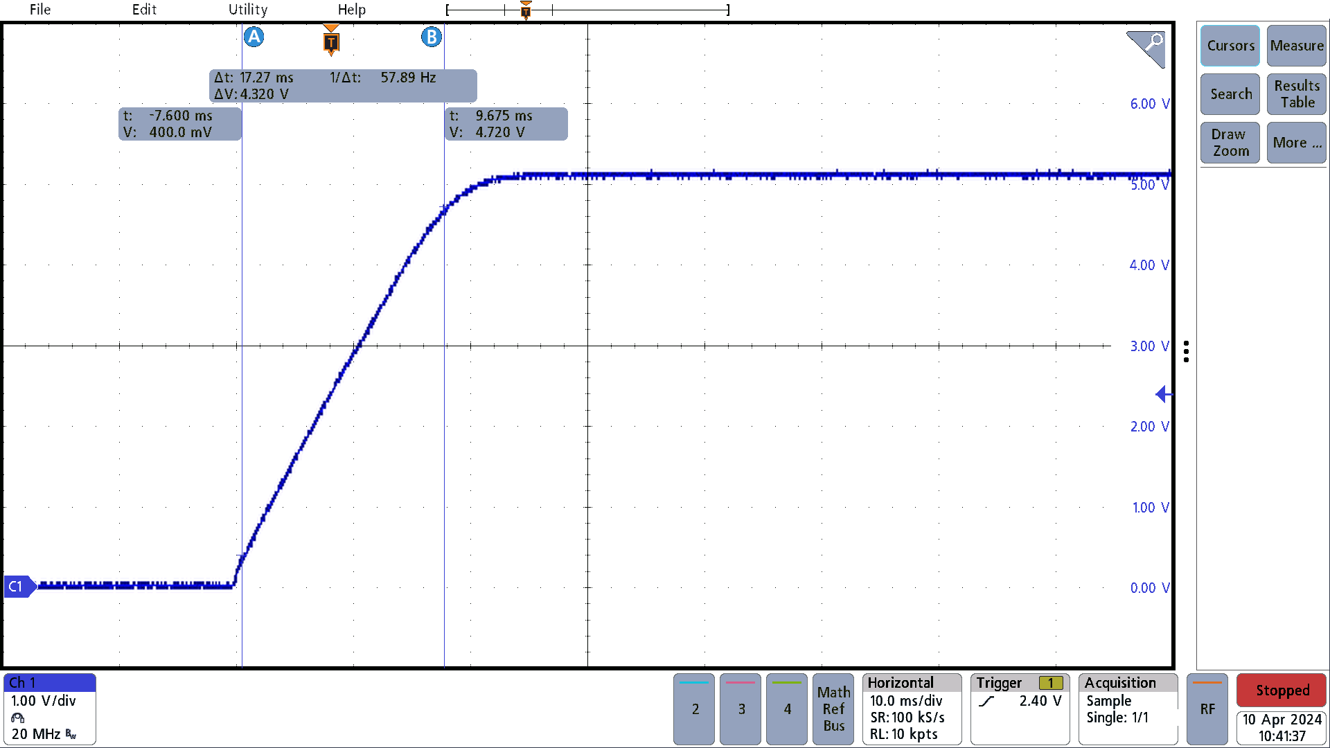
PMP23389 12V
                                                Input, 5.1V Output, No Load; CH1: Output Voltage,
                                                1V/divFigure 3-7 12V Input, 5.1V Output, No Load; CH1: Output Voltage, 1V/div
PMP23389 12V
                                                Input, 5.1V Output, 15A Maximum Load; CH1: Output
                                                Voltage, 1V/divFigure 3-8 12V Input, 5.1V Output, 15A Maximum Load; CH1: Output Voltage, 1V/div