TIDT399 July 2024
3.1 Switching
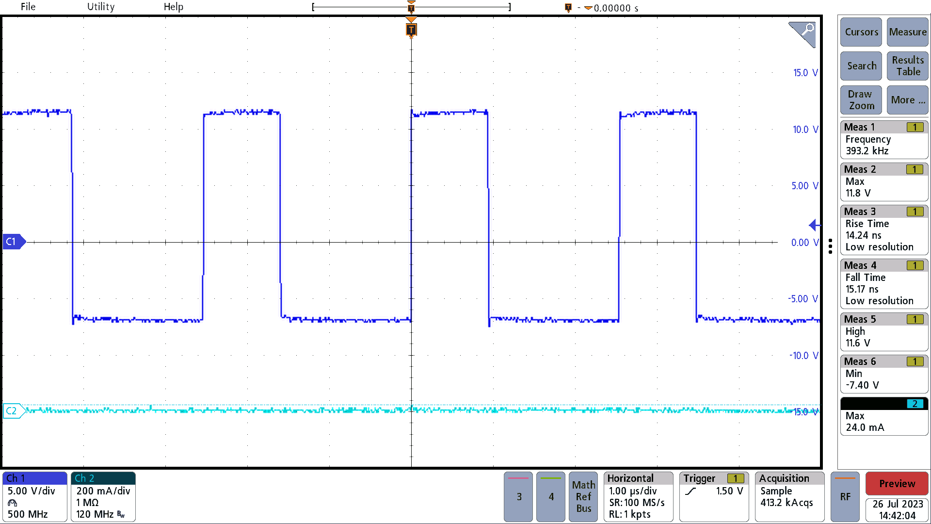
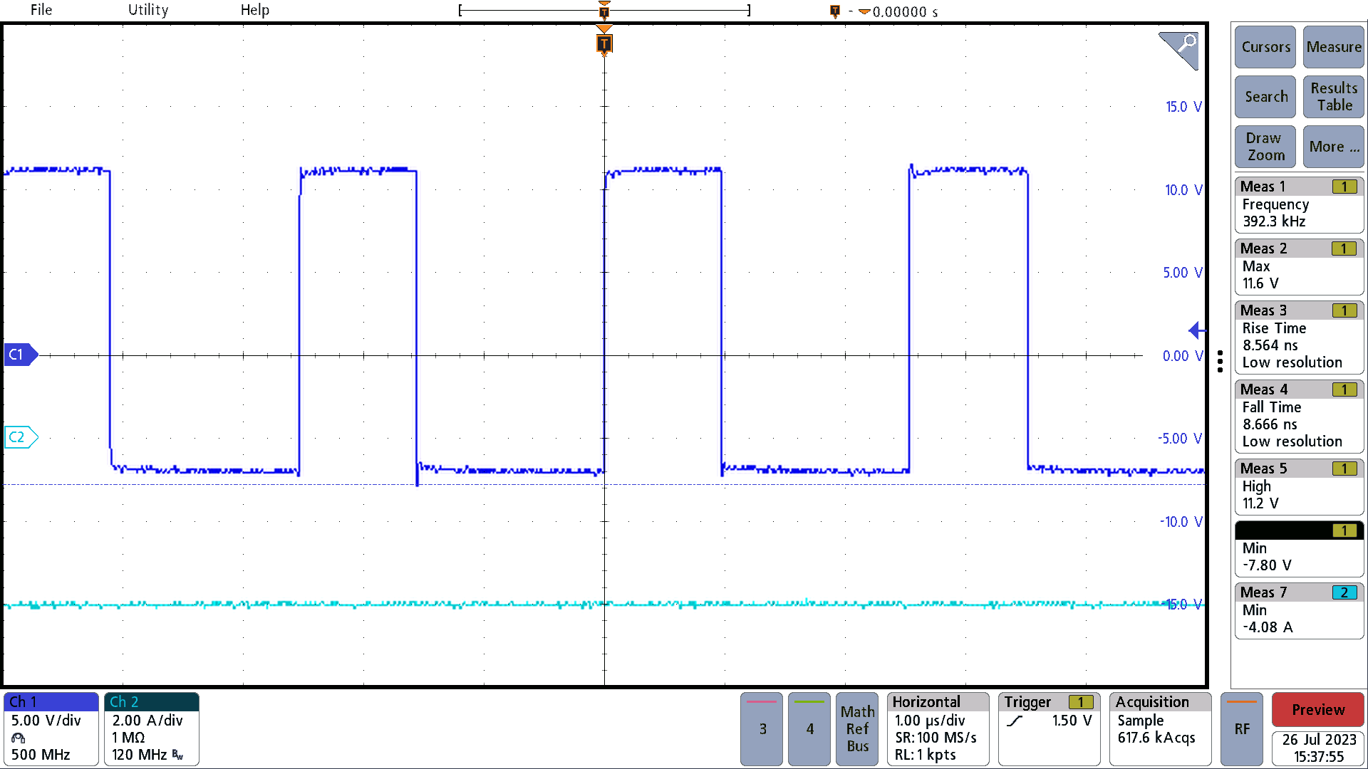
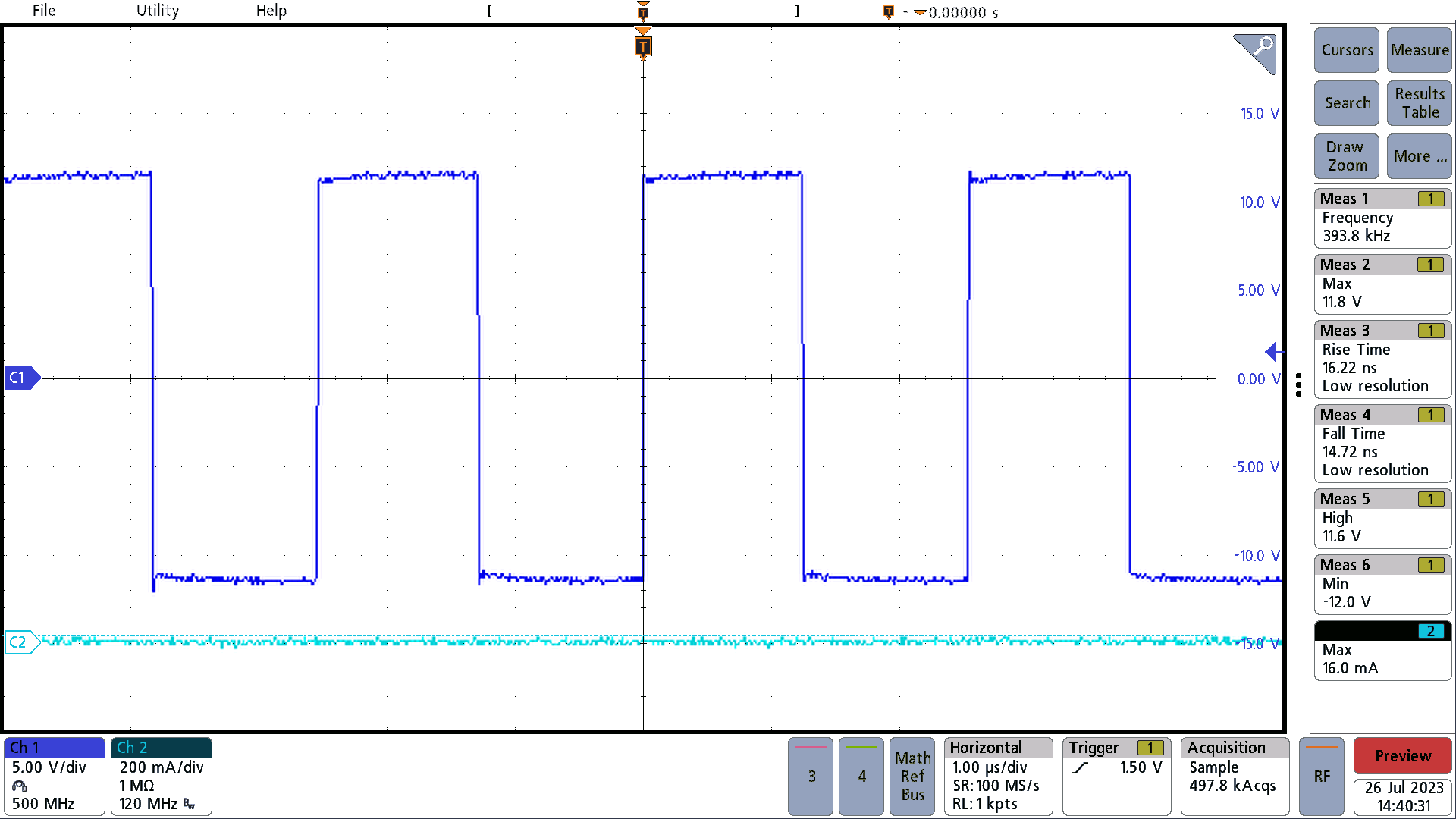
Figure 3-1 through Figure 3-4 show the switch node voltage waveforms of the converter at 12V input and –7.5V and –12V output at no load and 4A load conditions.
 Figure 3-1 Switch Node Voltage, 12V
Input, –7.5V Output, No Load
 Figure 3-2 Switch Node Voltage, 12V
Input, –7.5V Output, 4A Load
 Figure 3-3 Switch Node Voltage, 12V
Input, –12V Output, No Load
 Figure 3-4 Switch Node Voltage, 12V
Input, –12V Output, 4A Load