TIDU858C March   2015  – May 2021


  1.   Description
  2.   Resources
  3.   Features
  4.   Applications
  5.   5
  6. 1System Description
    1. 1.1 Binary Inputs or Digital Inputs
      1. 1.1.1 Binary Input Application Functionality
      2.      Common Specifications
    2. 1.2 Approaches to Binary Input Module Design
      1. 1.2.1 ADC Versus MCU Based Binary Input Module (BIM)
    3. 1.3 Measurement of Wide Inputs With Programmable Thresholds
  7. 2Design Features
    1. 2.1 Electrical Specifications
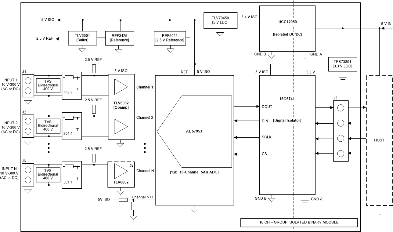
    2. 2.2 Block Diagram
      1. 2.2.1 Analog-to-Digital Converter (ADC)
        1. 2.2.1.1 ADS795x SAR ADC Family
      2. 2.2.2 Protection and Signal Conditioning
      3. 2.2.3 Digital Isolator
        1. 2.2.3.1 Host (SPI) Interfacing Using the ISO6741
      4. 2.2.4 DC Power Supply Isolator
      5. 2.2.5 Design Alternative: ADC With Digitally Programmable Threshold
        1. 2.2.5.1 ADS7128 SAR ADC With Programmable Threshold
        2. 2.2.5.2 I2C Interfacing Using the ISO1640 and Optional Altert Interface Using ISO7710
  8. 3Circuit Design and Component Selection
    1. 3.1 Analog-to-Digital Converter (ADC)
    2. 3.2 Input Signal Conditioning
      1. 3.2.1 Voltage Divider
      2. 3.2.2 TLV6002 Operational Amplifier
    3. 3.3 Isolated Interface
    4. 3.4 Isolated DC Power Supply
      1. 3.4.1 Reinforced Power Isolator: UCC12050 High-Efficiency 500-mW DC/DC Converter
    5. 3.5 Enhancements
  9. 4Testing
    1. 4.1 Test Setup and Connection Diagram
    2. 4.2 Test Data
      1. 4.2.1 Voltage Measurement Accuracy Testing
    3. 4.3 Test Results Summary
  10. 5Design Files
    1. 5.1 Schematics
    2. 5.2 Bill of Materials
    3. 5.3 Altium Project
    4. 5.4 Gerber Files
  11. 6References
  12.   Trademarks
  13. 7About the Author
  14. 8Revision History

GUID-20210407-CA0I-W9WB-9BC5-DD2MJCBVGKX9-low.gif
GUID-20210322-CA0I-77KX-QBSZ-DBN8NKMNBG2R-low.jpg