TIDUD61E October   2020  – April 2021


  1.   Description
  2.   Resources
  3.   Features
  4.   Applications
  5.   5
  6. 1System Description
    1. 1.1 Key System Specifications
  7. 2System Overview
    1. 2.1 Block Diagram
    2. 2.2 Design Considerations
      1. 2.2.1 Input AC Voltage Sensing
      2. 2.2.2 Bus Voltage Sensing
      3. 2.2.3 AC Current Sensing
      4. 2.2.4 Sense Filter
      5. 2.2.5 Protection (CMPSS)
    3. 2.3 Highlighted Products
      1. 2.3.1 C2000™ MCU F28004x
      2. 2.3.2 LMG3410R070
      3. 2.3.3 UCC27714
    4. 2.4 System Design Theory
      1. 2.4.1 PWM
      2. 2.4.2 Current Loop Model (PFC and Inverter mode)
      3. 2.4.3 DC Bus Regulation Loop (for PFC mode only)
      4. 2.4.4 Soft Start Around Zero Crossing for Eliminate or Reduce Current Spike
      5. 2.4.5 AC Drop Test
  8. 3Hardware, Software, Testing Requirements, and Test Results
    1. 3.1 Required Hardware and Software
      1. 3.1.1 Hardware
        1. 3.1.1.1 Base Board Settings
        2. 3.1.1.2 Control Card Settings
      2. 3.1.2 Software
        1. 3.1.2.1 Opening Project Inside CCS
        2. 3.1.2.2 Project Structure
        3. 3.1.2.3 Using CLA on C2000 MCU to Alleviate CPU Burden
        4. 3.1.2.4 CPU and CLA Utilization and Memory Allocation
        5. 3.1.2.5 Running the Project
          1. 3.1.2.5.1 Lab 1: Open Loop, DC (PFC Mode)
            1. 3.1.2.5.1.1 Setting Software Options for LAB 1
            2. 3.1.2.5.1.2 Building and Loading Project
            3. 3.1.2.5.1.3 Setup Debug Environment Windows
            4. 3.1.2.5.1.4 Using Real-Time Emulation
            5. 3.1.2.5.1.5 Running Code
          2. 3.1.2.5.2 Lab 2: Closed Current Loop DC (PFC)
            1. 3.1.2.5.2.1 Setting Software Options for Lab 2
            2. 3.1.2.5.2.2 Designing Current Loop Compensator
            3. 3.1.2.5.2.3 Building and Loading Project and Setting up Debug
            4. 3.1.2.5.2.4 Running Code
          3. 3.1.2.5.3 Lab 3: Closed Current Loop, AC (PFC)
            1. 3.1.2.5.3.1 Setting Software Options for Lab 3
            2. 3.1.2.5.3.2 Building and Loading Project and Setting up Debug
            3. 3.1.2.5.3.3 Running Code
          4. 3.1.2.5.4 Lab 4: Closed Voltage and Current Loop (PFC)
            1. 3.1.2.5.4.1 Setting Software Options for Lab 4
            2. 3.1.2.5.4.2 Designing Voltage Loop Compensator
            3. 3.1.2.5.4.3 Building and Loading Project and Setting up Debug
            4. 3.1.2.5.4.4 Running Code
          5. 3.1.2.5.5 Lab 5: Open loop, DC (Inverter)
            1. 3.1.2.5.5.1 Setting Software Options for Lab 5
            2. 3.1.2.5.5.2 Building and Loading Project
            3. 3.1.2.5.5.3 Setup Debug Environment Windows
            4. 3.1.2.5.5.4 Running Code
          6. 3.1.2.5.6 Lab 6: Open loop, AC (Inverter)
            1. 3.1.2.5.6.1 Setting Software Options for Lab 6
            2. 3.1.2.5.6.2 Building and Loading Project and Setting up Debug
            3. 3.1.2.5.6.3 Running Code
          7. 3.1.2.5.7 Lab 7: Closed Current Loop, DC (Inverter with resistive load)
            1. 3.1.2.5.7.1 Setting Software Options for Lab 7
            2. 3.1.2.5.7.2 Designing Current Loop Compensator
            3. 3.1.2.5.7.3 Building and Loading Project and Setting up Debug
            4. 3.1.2.5.7.4 Running Code
          8. 3.1.2.5.8 Lab 8: Closed Current Loop, AC (Inverter with resistive load)
            1. 3.1.2.5.8.1 Setting Software Options for Lab 8
            2. 3.1.2.5.8.2 Building and Loading Project and Setting up Debug
            3. 3.1.2.5.8.3 Running Code
          9. 3.1.2.5.9 Lab 9: Closed Current Loop (Grid Connected Inverter)
            1. 3.1.2.5.9.1 Setting Software Options for Lab 9
            2. 3.1.2.5.9.2 Building and Loading Project and Setting up Debug
            3. 3.1.2.5.9.3 Running Code: Emulated Grid-tied Condition (Verification purpose only)
            4. 3.1.2.5.9.4 Running Code: Grid-tied Condition
        6. 3.1.2.6 Running Code on CLA
        7. 3.1.2.7 Advanced Options
          1. 3.1.2.7.1 Input Cap Compensation for PF Improvement Under Light Load
          2. 3.1.2.7.2 83
          3. 3.1.2.7.3 Adaptive Dead Time for Efficiency Improvements
          4. 3.1.2.7.4 Phase Shedding for Efficiency Improvements
          5. 3.1.2.7.5 Non-Linear Voltage Loop for Transient Reduction
          6. 3.1.2.7.6 Software Phase Locked Loop Methods: SOGI - FLL
    2. 3.2 Testing and Results
      1. 3.2.1 Test Results at Input 120 Vrms, 60 Hz, Output 380-V DC
        1. 3.2.1.1 Startup
        2. 3.2.1.2 Steady State Condition
        3. 3.2.1.3 Transient Test With Step Load Change
          1. 3.2.1.3.1 0% to 50% Load Step Change
          2. 3.2.1.3.2 50% to 100% Load Step Change
          3. 3.2.1.3.3 100% to 50% Load Step Change
          4. 3.2.1.3.4 50% to 100% Load Step Change
      2. 3.2.2 Test Results at Input 230 Vrms, 50 Hz, Output 380 V DC
        1. 3.2.2.1 Startup
        2. 3.2.2.2 Steady State Condition
        3. 3.2.2.3 Transient Test With Step Load Change
          1. 3.2.2.3.1 33% to 100% Load Step Change
          2. 3.2.2.3.2 100% to 33% Load Step Change
      3. 3.2.3 Test Results Graphs
  9. 4Design Files
    1. 4.1 Schematics
    2. 4.2 Bill of Materials
    3. 4.3 PCB Layout Recommendations
      1. 4.3.1 Layout Prints
    4. 4.4 Altium Project
    5. 4.5 Gerber Files
    6. 4.6 Assembly Drawings
  10. 5Software Files
  11. 6Related Documentation
    1. 6.1 Trademarks
  12. 7About the Author
  13. 8Revision History
Input Cap Compensation for PF Improvement Under Light Load

Input cap causes PF degradation if the current reference is maintained perfectly in sync with the voltage as shown in Equation 8 and in Figure 3-46(a).

Equation 8. GUID-969CAE35-96B0-4884-B3B9-B202AB5628ED-low.gif

The current reference can be adjusted with vectors to offset the PF degradation, Equation 9, Figure 3-46(b) . As the angle from the phase locked loop is used to compute the vector this technique is called the digital phase locked loop vector cancellation (DPLLVC) technique. This improves PF at light load and high line significantly.

Equation 9. GUID-CDADDCC3-2040-4CF8-A018-B0217762164B-low.gif

The amount of correction applied depends on the input capacitor value, for example on this design the input cap is 2.2 µF. Which means at high line a capacitive current equal to GUID-79FDCFD8-BA37-4296-A3A0-589FC9E168F5-low.gif 
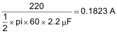
is drawn. Under light loads, this is significant amount of current and causes power factor loss. The current sensor gain on this design is approximately 24 A, so this translates to an adjustment of approximately 0.01 pu for the high-line condition.

Furthermore, there is a tracking error under low power conditions. This tracking error can be offset by an adjustment to the current command shown in Figure 3-46©). The amount of this tracking error is adjusted empirically for the best performance from the system. Thus the total current reference is given by Equation 10.

Equation 10. GUID-B245AB56-5AC1-44A9-BB8D-73EE74193A6B-low.gif
GUID-4529F7F5-A8D6-40F7-B790-F93F864D8DCB-low.gifFigure 3-46 Power Factor (a) No Adjustment (b) DPLLVC ©) DPLLVC Plus Tracking Error Compensation

The result for PF improvement are graphed in Figure 3-47.

GUID-519688ED-CEB2-4FB0-8304-5A694279F759-low.gifFigure 3-47 PF Graph vs Power at 220 Vrms Highlighting Improvement With Input Cap Current Compensation