TIDUD61E October 2020 – April 2021
- Description
- Resources
- Features
- Applications
- 5
- 1System Description
- 2System Overview
-
3Hardware, Software, Testing Requirements, and Test Results
- 3.1
Required Hardware and Software
- 3.1.1 Hardware
- 3.1.2
Software
- 3.1.2.1 Opening Project Inside CCS
- 3.1.2.2 Project Structure
- 3.1.2.3 Using CLA on C2000 MCU to Alleviate CPU Burden
- 3.1.2.4 CPU and CLA Utilization and Memory Allocation
- 3.1.2.5
Running the Project
- 3.1.2.5.1 Lab 1: Open Loop, DC (PFC Mode)
- 3.1.2.5.2 Lab 2: Closed Current Loop DC (PFC)
- 3.1.2.5.3 Lab 3: Closed Current Loop, AC (PFC)
- 3.1.2.5.4 Lab 4: Closed Voltage and Current Loop (PFC)
- 3.1.2.5.5 Lab 5: Open loop, DC (Inverter)
- 3.1.2.5.6 Lab 6: Open loop, AC (Inverter)
- 3.1.2.5.7 Lab 7: Closed Current Loop, DC (Inverter with resistive load)
- 3.1.2.5.8 Lab 8: Closed Current Loop, AC (Inverter with resistive load)
- 3.1.2.5.9 Lab 9: Closed Current Loop (Grid Connected Inverter)
- 3.1.2.6 Running Code on CLA
- 3.1.2.7
Advanced Options
- 3.1.2.7.1 Input Cap Compensation for PF Improvement Under Light Load
- 3.1.2.7.2 83
- 3.1.2.7.3 Adaptive Dead Time for Efficiency Improvements
- 3.1.2.7.4 Phase Shedding for Efficiency Improvements
- 3.1.2.7.5 Non-Linear Voltage Loop for Transient Reduction
- 3.1.2.7.6 Software Phase Locked Loop Methods: SOGI - FLL
- 3.2 Testing and Results
- 3.1
Required Hardware and Software
- 4Design Files
- 5Software Files
- 6Related Documentation
- 7About the Author
- 8Revision History
3.2.2.2 Steady State Condition
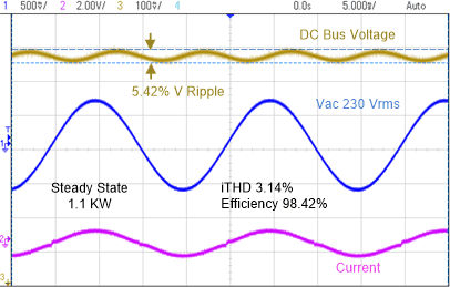
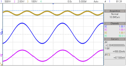
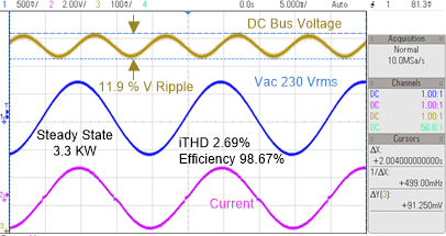
Figure 3-74, Figure 3-75, and Figure 3-76 show the steady state current waveform at different load conditions. Phase shedding is disabled for these readings.
 Figure 3-74 Steady State 230-Vac IN, 380-V DC OUT, 1.1KW, iTHD 3.14%
 Figure 3-75 Steady State 230-Vac IN, 380-V DC OUT, 2.2KW, iTHD 2.62%
 Figure 3-76 Steady State 230-Vac IN, 380-V DC OUT, 3.3KW, iTHD 2.69%
Table 3-4 lists the detailed test results of this design under varying load conditions with 230-Vac input and 380-V DC output. For the following data, phase shedding is disabled, adaptive dead time is enabled, 100 ns is chosen as the fixed dead time for the hard switched edge, and the soft-switching edge dead time varies between 20 ns to 200 ns.
Table 3-4 Detailed Test Results With 230-Vac IN, 380-V DC OUT and Different Power Levels
| Vin (V RMS) | Vout (V) | Pin (W) | Iout (A) | Pout (W) | EFFICIENCY % | iTHD% | PF | % RATED LOAD | THETA OFFSET | Gi Kp |
|---|---|---|---|---|---|---|---|---|---|---|
| 230.68 | 381.98 | 151.28 | 0.372 | 142.16 | 94.03 | 18.20 | 0.9775 | 4.4 | -0.025 | 0.35 |
| 230.43 | 382.00 | 292.24 | 0.736 | 281.41 | 96.29 | 9.15 | 0.9936 | 8.8 | -0.02 | 0.35 |
| 230.25 | 382.03 | 435.90 | 1.109 | 423.62 | 97.18 | 6.12 | 0.9938 | 13.2 | -0.01 | 0.35 |
| 230.06 | 382.06 | 576.40 | 1.473 | 562.86 | 97.66 | 4.85 | 0.9972 | 17.6 | -0.01 | 0.35 |
| 229.80 | 382.05 | 856.80 | 2.201 | 841.00 | 98.15 | 4.16 | 0.9974 | 26.3 | 0 | 0.35 |
| 229.70 | 382.11 | 1140.10 | 2.935 | 1121.90 | 98.42 | 3.14 | 0.9989 | 35.1 | 0 | 0.35 |
| 229.52 | 382.08 | 1418.80 | 3.659 | 1398.40 | 98.57 | 2.42 | 0.9993 | 43.7 | 0 | 0.3 |
| 229.28 | 382.08 | 1699.20 | 4.386 | 1676.40 | 98.66 | 2.74 | 0.9995 | 52.4 | 0 | 0.3 |
| 229.06 | 382.09 | 1977.70 | 5.106 | 1951.90 | 98.71 | 2.56 | 0.9996 | 61.0 | 0 | 0.3 |
| 229.09 | 382.11 | 2261.50 | 5.840 | 2232.40 | 98.73 | 2.62 | 0.9995 | 69.8 | 0 | 0.25 |
| 228.91 | 382.11 | 2548.30 | 6.580 | 2515.60 | 98.73 | 2.50 | 0.9994 | 78.6 | 0 | 0.25 |
| 228.86 | 382.14 | 2840.60 | 7.332 | 2803.20 | 98.71 | 2.89 | 0.9990 | 87.6 | 0 | 0.2 |
| 228.51 | 382.12 | 3132.80 | 8.083 | 3091.10 | 98.69 | 2.80 | 0.9989 | 96.6 | 0 | 0.2 |
| 228.22 | 382.03 | 3439.10 | 8.873 | 3392.30 | 98.65 | 2.69 | 0.9988 | 106.0 | 0 | 0.2 |