TIDUEB8C July 2018 – March 2021 TPS274160
- Description
- Resources
- Features
- Applications
- 5
- 1System Description
- 2System Overview
- 3Hardware, Software, Testing Requirements, and Test Results
- 4Design Files
- 5Software Files
- 6Related Documentation
- 7About the Author
- 8Revision History
3.2.2.4 Residue Voltage
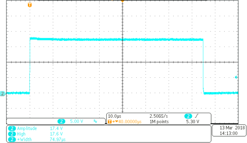
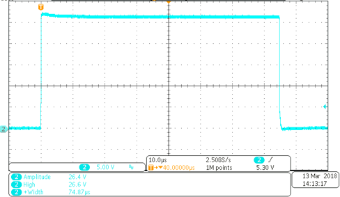
The test case TCM_PHYL_INTF_IQPKHM tests the voltage drop on the high side of the IO-Link PHY during the wake-up pulse. Therefore the CQ line is loaded with 26 Ω and the wake-up pulse is generated. The voltage on the CQ line has to exceed 13 V to pass this test. This test is done with a L+ voltage of 20 V and 30 V.
 Figure 3-8 Testcase TCM_PHYL_INTF_IQPKHM: Wake-Up Current High Side - 20 V L+ Resulting in 17.4 V
 Figure 3-9 Testcase TCM_PHYL_INTF_IQPKHM: Wake-Up Current High Side - 30 V L+ Resulting in 26.4 V
As Figure 3-8 and Figure 3-9 show, the voltage is above 13 V, so the test of the high-side driver is passed.
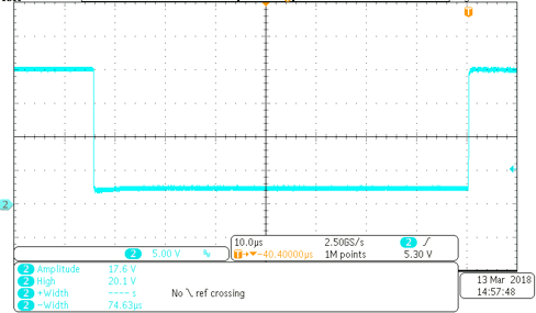
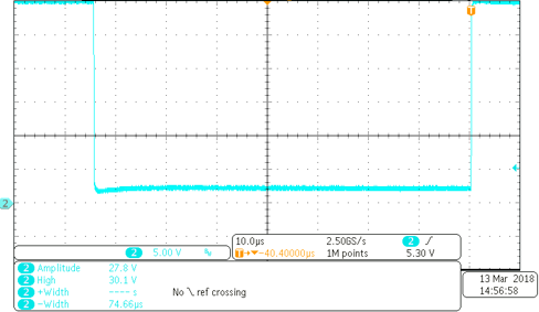
The next relevant test case is TCM_PHYL_INTF_IQPKLM. This test is similar than before, but testing the low-side switch. Therefore the load is 24 Ω for 20 V L+ voltage and 44 Ω for 30 V. The resistor must be connected between L+ and CQ to test the low side. The voltage has to be below 8 V to pass this test.
 Figure 3-10 Testcase TCM_PHYL_INTF_IQPKLM: Wake-Up Current Low Side - 20 V L+ Resulting in 2 V
 Figure 3-11 Testcase TCM_PHYL_INTF_IQPKLM: Wake-Up Current Low Side - 30 V L+ Resulting in 2 V
So all the tests for the current capability during the wake-up pulse are passed.