TIDUEO0C July 2019 – March 2021
- Description
- Resources
- Features
- Applications
- 5
- 1System Description
-
2System Overview
- 2.1 Block Diagram
- 2.2 Design Considerations
- 2.3
Highlighted Products
- 2.3.1 TPS63900: 1.8V-5.5 VIN Buck-Boost Converter With 75-nA Ultra-low Quiescent Current and 400-mA Output Current
- 2.3.2 TPS610995: 0.7 VIN Synchronous Boost Converter With 400-nA Ultra-low Quiescent Current and 1-A Peak Current
- 2.3.3 TPS62840: 750-mA Synchronous Step-Down Converter With Ultra-low Quiescent Current Consumption
- 2.4 System Design Theory
- 3Hardware, Software, Testing Requirements, and Test Results
- 4Design Files
- 5Software Files
- 6Related Documentation
- 7Terminology
- 8About the Author
- 9Revision History
3.2.1 Test Setup
Two different test setups were used in order to take data with the three power devices. The TPS62840 and the TPS610995 are both integrated into the TIDA-010053 board while the other test setup was done using the TPS63900EVM.
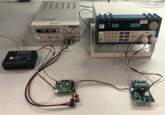
For the TPS610995 and TPS62840 setup, two in-series or one individual FDK battery (see the FDK CR17500EP Data Sheet) were soldered to the TIDA-010053 design and wired as in Figure 3-5 to the TIDA-01546 battery monitoring system. Then, using the BQ Studio GUI software, the BQ35100 primary cell battery gauge was configured and calibrated.

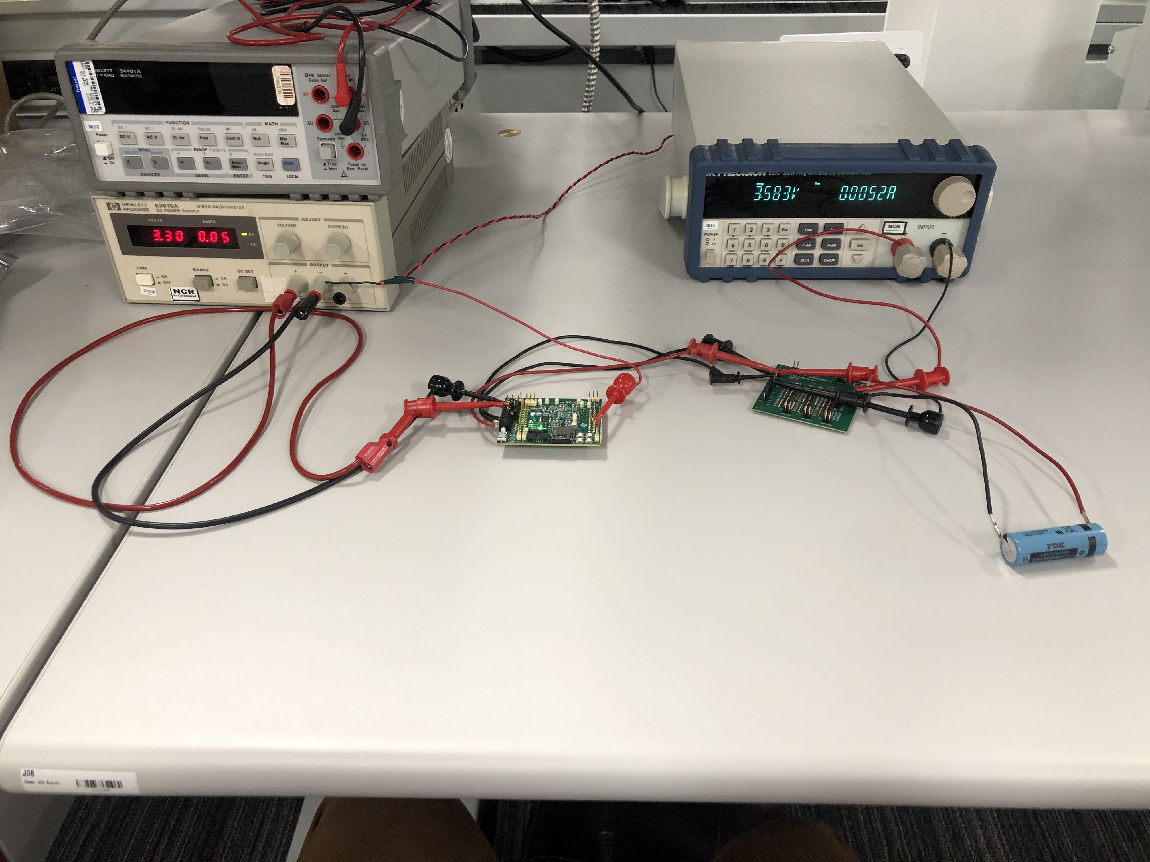
For the TPS63900 setup, one FDK battery was soldered to the input terminal of the TPS63900EVM and wired to the TIDA-01546 battery monitoring system as shown in Figure 3-6. The gauge was calibrated in the same way as the previous setup. Note that the TPS63900 EVM is the board shown on the right.
 Figure 3-6 TPS63900 Setup with TIDA-01546.
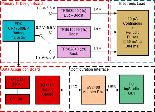
 Figure 3-7 shows the lab bench device configuration.
 Figure 3-7 Test Setup Block Diagram
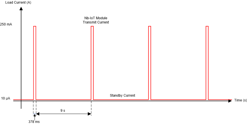
Figure 3-7 shows the load profile used by the Electronic Load to test.
 Figure 3-8 User Load Profile to Estimate Nb-IoT Module Current Consumption
- Transmit RF: 250 mA for 384 ms (1 pulse × 30 s or 1 pulse × 10 s)
- Metrology mode: 10-µA continuous base load
In addition to the electronic load for transmission emulation, metrology mode was represented through load resistors, which were connected to VOUT of the buck, buck-boost, and boost solutions. The TPS device currents, IOUT, were measured to be 10 µA, representing the 5- to 6-µA average current drawn in stand-by in many applications plus the 4 µA for power-save mode for the NB-IoT modules, see Section 2.4.3.
Using TIDA-01546, the onboard BQ35100 device was configured through the J18 I2C connector, then programmed using an EV2400 and a PC with BQ Studio GUI software installed. The ChemID = 0x635 was loaded to the device for the FDK CR17500EP cells and either the 2s or 1s cell configuration was selected. Additionally, jumpers J1 and J2 were set to the 2s or 1s configuration on the TIDA-01546 board, depending on the device under test. The ambient temperature of 21°C and the voltage offset were calibrated using a digital thermometer and digital multimeter, as reference. Furthermore, all devices used – besides the power managment devices – were powered through an external 3.3-V power supply. This was done to isolate the power consumption of the NB-IoT electronic load profile and the power converters.
The MCU on the TIDA-01546 was programmed to trigger an electronic load via GPIO, pulsing 250 mA for 384 ms. SOH and voltage data points were captured just prior to the next electronic load pulse, to ensure the voltage and SOH were most accurately reflected and maximizing available battery relaxation time. Additionally, the MCU issued a new battery command every cycle, such that the SOH captured was allowed to increase over time. This was done to capture raw data each cycle; however, in practice the new battery command would only be issued at the beginning of testing, preventing the SOH reading from increasing. This automated battery discharge and data collection set up ran throughout the entire lifetime of the primary cells.