TIDUEP0 May 2020
- Description
- Resources
- Features
- Applications
- 1Design Images
- 2System Description
-
3System Overview
- 3.1 Block Diagram
- 3.2 Design Considerations
- 3.3
Highlighted Products
- 3.3.1 TPD4E05U06 4-Channel Ultra-Low-Capacitance IEC ESD Protection Diode
- 3.3.2 TPD2EUSB30 2-Channel ESD Solution for SuperSpeed USB 3.0 Interface
- 3.3.3 2.3.3 HD3SS3220 10Gbps USB 3.1 USB Type-C 2:1 MUX With DRP Controller
- 3.3.4 TPS54218 2.95V to 6V Input, 2A Synchronous Step-Down SWIFT™ Converter
- 3.3.5 TPS54318 2.95V to 6V Input, 3A Synchronous Step-Down SWIFT™ Converter
- 3.3.6 CSD19538Q3A 100V, N ch NexFET MOSFET™, single SON3x3, 49mOhm
- 3.3.7 LM3488 2.97V to 40V Wide Vin Low-Side N-Channel Controller for Switching Regulators
- 3.3.8 TPS61178 20-V Fully Integrated Sync Boost with Load Disconnect
- 3.3.9 LMZM23601 36-V, 1-A Step-Down DC-DC Power Module in 3.8-mm × 3-mm Package
- 3.3.10 TPS7A39 Dual, 150mA, Wide-Vin, Positive and Negative Low-Dropout (LDO) Voltage Regulator
- 3.3.11 TPS74201 Single-output 1.5-A LDO regulator, adjustable (0.8V to 3.3V), any or no cap, programmable soft start
- 3.3.12 LP5910 300-mA low-noise low-IQ low-dropout (LDO) linear regulator
- 3.3.13 LP5907 250-mA ultra-low-noise low-IQ low-dropout (LDO) linear
- 3.3.14 INA231 28V, 16-bit, i2c output current/voltage/power monitor w/alert in wcsp
- 3.4
System Design Theory
- 3.4.1 Input Section
- 3.4.2
Designing of SEPIC based High Voltage Supply
- 3.4.2.1 Basic Operation Principle of SEPIC Converter
- 3.4.2.2 Design of Dual SEPIC Supply using uncoupled inductors
- 3.4.2.3 Duty Cycle
- 3.4.2.4 Inductor Selection
- 3.4.2.5 Power MOSFET Selection
- 3.4.2.6 Output Diode Selection
- 3.4.2.7 Coupling Capacitor Selection
- 3.4.2.8 Output Capacitor Selection
- 3.4.2.9 Input Capacitor Selection
- 3.4.2.10 Programming the Output Voltage
- 3.4.3 Designing the Low Voltage Power Supply
- 3.4.4 Designing the TPS54218 through Webench Power Designer
- 3.4.5 ± 5V Transmit Supply Generation
- 3.4.6 System Clock Synchronization
- 3.4.7 Power and data output connector
- 3.4.8 System Current and Power Monitoring
- 4Hardware, Software, Testing Requirements, and Test Results
- 5Layout Guidelines
- 6Design Files
- 7Software Files
- 8Related Documentation
- 9About the Author
3.1 Block Diagram

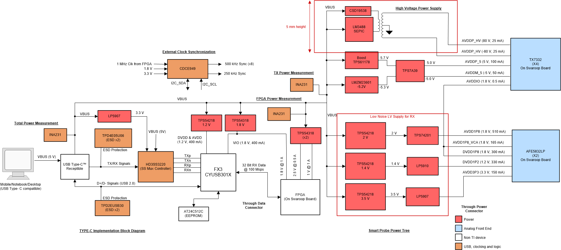
This design implements a full power tree solution that includes a single-stage transformer-less HV generation for transmit and the point-of-load LV for the AFEs and FPGA from a 5-V USB Type-C input. The entire implementation is divided into two sections, the high voltage power supply (SLOA284) and a low voltage supply. The system takes its input from a mobile phone, notebook, or desktop from a 5V USB Type-C. This 5V input is then used by different power management solutions used to power both the FPGA and the AFE5832LP and TX7332. In order to monitor the power consumption of various sub-systems in the design. For the low voltage supplies for both AFE5832LP and TX7332, each DC/DC converter is followed by an LDO to remove noise with a higher PSRR. Since the ultrasound smart probe is a noise sensitive design, the high PSRR is a key specification for an increase in image quality. The FPGA, USB controller, and clocking supply are powered by highly efffieint and low power solutions using the TPS54218 and the LP907. The FX3 device on the power supply board is programmed with USB Bulk Data Source Sink test to evaluate the speed of the data transfer The measured data speed is 4.2 Gbps which aligns with the expected value from the FX3 datasheet. Finally, there are INA231's to monitor the current of each power stage to ensure a higher performing operation.