TIDUEU6B
September 2020 – December 2021
OPA810
Description
Resources
Features
Applications
5
1
System Description
1.1
Key System Specifications
2
System Overview
2.1
Block Diagram
2.2
Highlighted Products
2.2.1
OPA2810
2.2.2
BUF634A
2.3
Design Considerations
2.3.1
Existing architecture
2.3.1.1
Circuit Stability Issue
2.3.1.2
Solution in Existing Architecture (Compensation Cap)
2.3.2
Proposed Design
2.3.2.1
Stability Analysis of the Proposed Design
2.3.2.1.1
Without Measurement of Voltage at Inverting Node of A2
2.3.2.1.2
With Measuring Voltage at Inverting Node of A2
2.3.2.2
RG = RF Settings and Respective Impedance Ranges
2.3.2.3
Impedance Measurement Procedure
2.3.2.3.1
Short Cal
2.3.2.3.2
Impedance Cal
2.3.2.3.3
100k Setting Calibration
2.3.2.3.4
Open Cal
2.3.2.3.5
Calculations
2.3.2.3.6
Correction in ZX
2.3.2.3.7
Data Acquisition and Processing
2.3.2.3.8
Mathematical Explanation
3
Hardware, Software, Testing Requirements, and Test Results
3.1
Required Hardware and Software
3.1.1
Hardware
3.2
Testing and Results
3.2.1
Test Setup
3.2.2
Test Results
4
Design Files
4.1
Schematics
4.2
Bill of Materials
4.3
PCB Layout Recommendations
4.3.1
Layout Prints
4.4
Altium Project
4.5
Gerber Files
4.6
Assembly Drawings
5
Software Files
6
Related Documentation
6.1
Trademarks
6.2
Third-Party Products Disclaimer
7
Revision History
2.1
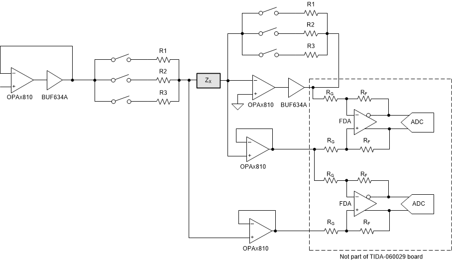
Block Diagram
Figure 2-1
TIDA-060029 Block Diagram