TIDUEU6B September   2020  – December 2021 OPA810


  1.   Description
  2.   Resources
  3.   Features
  4.   Applications
  5.   5
  6. 1System Description
    1. 1.1 Key System Specifications
  7. 2System Overview
    1. 2.1 Block Diagram
    2. 2.2 Highlighted Products
      1. 2.2.1 OPA2810
      2. 2.2.2 BUF634A
    3. 2.3 Design Considerations
      1. 2.3.1 Existing architecture
        1. 2.3.1.1 Circuit Stability Issue
        2. 2.3.1.2 Solution in Existing Architecture (Compensation Cap)
      2. 2.3.2 Proposed Design
        1. 2.3.2.1 Stability Analysis of the Proposed Design
          1. 2.3.2.1.1 Without Measurement of Voltage at Inverting Node of A2
          2. 2.3.2.1.2 With Measuring Voltage at Inverting Node of A2
        2. 2.3.2.2 RG = RF Settings and Respective Impedance Ranges
        3. 2.3.2.3 Impedance Measurement Procedure
          1. 2.3.2.3.1 Short Cal
          2. 2.3.2.3.2 Impedance Cal
          3. 2.3.2.3.3 100k Setting Calibration
          4. 2.3.2.3.4 Open Cal
          5. 2.3.2.3.5 Calculations
          6. 2.3.2.3.6 Correction in ZX
          7. 2.3.2.3.7 Data Acquisition and Processing
          8. 2.3.2.3.8 Mathematical Explanation
  8. 3Hardware, Software, Testing Requirements, and Test Results
    1. 3.1 Required Hardware and Software
      1. 3.1.1 Hardware
    2. 3.2 Testing and Results
      1. 3.2.1 Test Setup
      2. 3.2.2 Test Results
  9. 4Design Files
    1. 4.1 Schematics
    2. 4.2 Bill of Materials
    3. 4.3 PCB Layout Recommendations
      1. 4.3.1 Layout Prints
    4. 4.4 Altium Project
    5. 4.5 Gerber Files
    6. 4.6 Assembly Drawings
  10. 5Software Files
  11. 6Related Documentation
    1. 6.1 Trademarks
    2. 6.2 Third-Party Products Disclaimer
  12. 7Revision History

Hardware

Figure 3-1 and Figure 3-2 illustrate the schematic and board connections of the TIDA-060029 board.
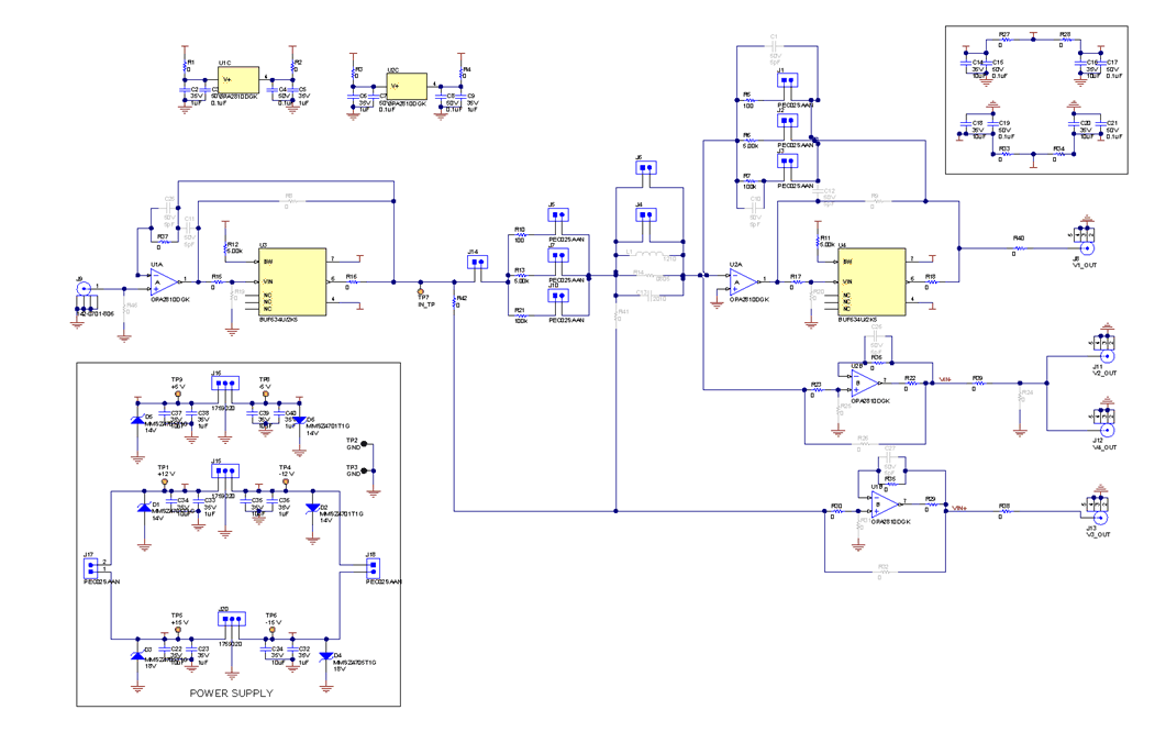
GUID-73F64AA8-D662-4A6B-9305-78892F03CBF5-low.gif Figure 3-1 Hardware Schematic
GUID-A4AC0B8E-E6D6-4567-AAAA-496ED26ABE0F-low.gifFigure 3-2 Board Connections
Table 3-1 Connector Details
CONNECTOR DESCRIPTION
J1, J2, J3, J5, J7, J10 RG = RF Settings connectors
J6 Offset Calibration connector
J14 Offset Cal Connector
J15 OPA2810 Supply
J20 BUF634 Supply
J16 VCA 821 Supply
J17, J18 Jumpers between J15 and J20
J9 Input Connector
J12, J13 VX Measurement Connectors
J8, J11 VOUT Measurement Connectors