TIDUEW7 May 2020
- Description
- Resources
- Features
- Applications
- Design Images
- 1System Description
-
2System Overview
- 2.1 Block Diagram
- 2.2 Design Considerations
- 2.3 Highlighted Products
- 2.4 System Design Theory
- 3Getting Started, Testing Setup, and Test Results
- 4Design Files
- 5Software Files
- 6Related Documentation
2.4.2 Power Sequencing
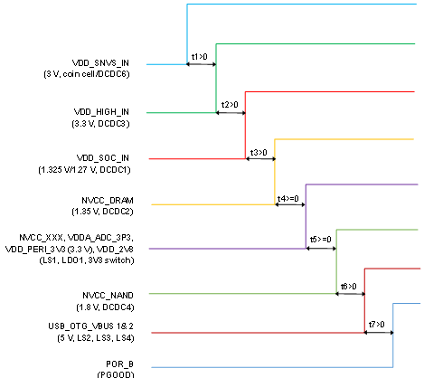
The processor power-up sequencing is shown in Figure 16. First the VDD_SNVS needs to turn on before any other power supply. For our design, VDD_SNVS is powered through a coin cell connected to the CC pin of the TPS6521815 PMIC, and the DCDC6 supply will always be the first PMIC supply rail to turn on. Once SNVS voltage is stabilized, then VDD_HIGH_IN should turn on because VDD_HIGH_IN should be enabled before VDD_SOC_IN for the i.MX 6ULL processor. After VDD_SOC_IN, NVCC_DRAM is turned on for the DDR3L memory followed by 3.3 V for I/O and analog along with 2.8 V for the LCD screen. The final supply to turn on is the 1.8-V I/O rail. Once all these voltages are enabled and within regulation, there is a delay before PGOOD is set high. PGOOD is the PMIC output that control the power-on reset (POR_B) input of the processor.
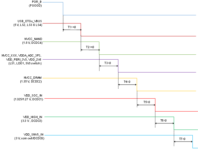
The processor power-down sequencing is shown in Figure 17, which is the reverse of the power-up sequence.

