TIDUEZ0A March   2021  – March 2022 TMS320F28P550SJ , TMS320F28P559SJ-Q1


  1.   Description
  2.   Resources
  3.   Features
  4.   Applications
  5.   5
  6. 1System Description
    1. 1.1 Key System Specifications
  7. 2System Overview
    1. 2.1 Block Diagram
    2. 2.2 Design Considerations
      1. 2.2.1 Three-Phase ANPC Inverter Architecture Overview
      2. 2.2.2 LCL Filter Design
      3. 2.2.3 Power Switching Devices Selection
      4. 2.2.4 GaN Power Stage
      5. 2.2.5 Voltage Sensing
      6. 2.2.6 Current Sensing
      7. 2.2.7 System Power Supplies
        1. 2.2.7.1 Isolated Bias Supplies
      8. 2.2.8 Si Gate Driver Circuit
  8. 3Hardware, Software, Testing Requirements, and Test Results
    1. 3.1 Hardware and Software Requirements
      1. 3.1.1 Hardware
      2. 3.1.2 Software
    2. 3.2 Testing TIDA-010210 With AC Resistive Load
      1. 3.2.1 Test Setup
      2. 3.2.2 Experimental Results
    3. 3.3 Testing TIDA-010210 in PFC Operation
      1. 3.3.1 Test Setup
      2. 3.3.2 Experimental Results
  9. 4Design and Documentation Support
    1. 4.1 Design Files
      1. 4.1.1 Schematics
      2. 4.1.2 BOM
      3. 4.1.3 Altium Project
      4. 4.1.4 Gerber Files
      5. 4.1.5 Assembly Drawings
    2. 4.2 Tools and Software
    3. 4.3 Support Resources
    4. 4.4 Trademarks
  10. 5About the Authors
  11. 6Revision History

Experimental Results

The open loop test output waveforms in Figure 3-2 show clean sinusoidal waveforms with the new PWM scheme, when DC bus is operating at 800 V. There is very little distortion even at zero crossing with CLB based protection active.
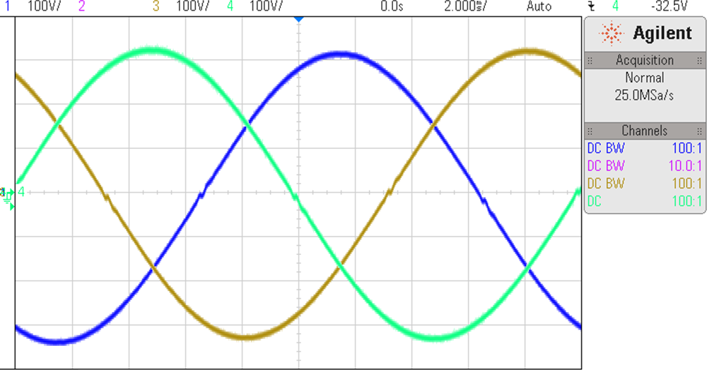
GUID-20210218-CA0I-G0JZ-0T0V-Q17JZDCCQDDV-low.pngFigure 3-2 Open Loop Output Waveforms (AC Load Voltage Waveforms)

The current loop stability of the circuit is demonstrated by the smooth transition in the current transient response. Figure 3-3 shows the response when current is changed from 1 A to 6 A and Figure 3-4 shows the response when current is changed from 6 A to 1 A.
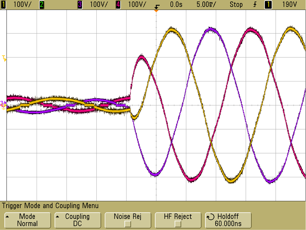
GUID-20210218-CA0I-DKPZ-9HB4-NNN2FRFKHQST-low.png Figure 3-3 Positive-Going Transient Response (AC Load Voltage Waveforms)
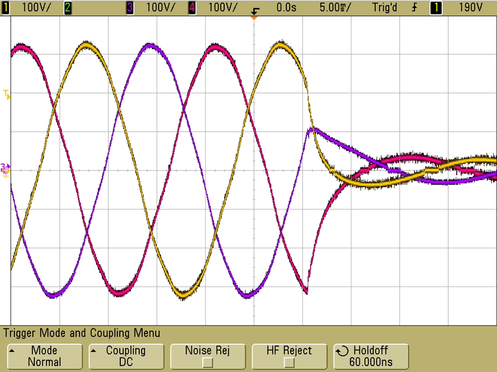
GUID-20210218-CA0I-NPTQ-LW3N-MWD99X3FXRHN-low.png Figure 3-4 Negative-Going Transient Response (AC Load Voltage Waveforms)