TIDUEZ0A March 2021 – March 2022 TMS320F28P550SJ , TMS320F28P559SJ-Q1
2.2.2 LCL Filter Design
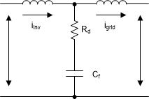
Any system of power transfer with the grid is required to meet certain output specifications for harmonic content. In many rectifiers, a high-order LCL filter typically provides sufficient harmonic attenuation, along with reducing the overall design size versus a simpler filter design. However, due to the higher order nature, take some care in its design to control resonance. Figure 2-8 shows a typical LCL filter.
 Figure 2-8 LCL Filter Architecture
One of the key benefits of using GaN switching device (as this reference design does) is the ability to increase the switching frequency of the power stage significantly versus traditional Si-based switching devices. This increased switching frequency has a direct impact on the filter resonant design of the converter, which needs to be accounted for. To ensure that the filter is designed correctly around this switching frequency, the known mathematical model of this type of filter is used in this design.
The primary component is the switch side inductor, or Linv, which can be derived using Equation 1:

Using the system specifications, the primary inductor value can be calculated:

An inductor from Wurth Elektronik (750344413) with rated current of 15 A having zero bias inductance of 480 mH is used. With the high current bias during the operation, the inductance can reduce by 25% as per the data sheet. This results in an effective inductance of 360 mH at 15 A, which is sufficient to ensure ripple current below 40%.
The sizing of the primary filter capacitor is handled in a similar fashion using Equation 3:

Make some design assumptions to finalize the value of Cf , limiting the total reactive power absorbed by the capacitor to 3.5%. Scaling the total system power by the per phase power results in a primary capacitor value of:

A standard value capacitor of 4.7 μF was selected.
For the remainder of the filter design, determine the values by defining the attenuation factor between the allowable ripple in grid inductor and the inverter inductor. This factor needs to be minimized while still maintaining a stable and cost effective total filter. By assuming an attenuation factor, an r value, which defines the ratio between the two inductors, is determined using Equation 5:

Where Cb is given by:

To obtain an attenuation factor of 5%, and using the earlier derived values, the value of r can be evaluated by rewriting Equation 5 to be:

The resultant value for Lgrid is then:

A higher standard value of 15 μH was selected to ensure good attenuation.
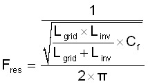
The filter design can be validated by determining its resonant frequency (Fres). A good criteria for ensuring a stable Fres is that it is an order of magnitude above the line frequency and less than half the switching frequency. This criteria avoids issues in the upper and lower harmonic spectrums. The resonant frequency of the filter is given by Equation 9:

Using the derived filter values, the resonant frequency is:

This value for Fres meets the criteria listed earlier and validates the filter design.
The remaining value to determine is the passive damping that must be added to avoid oscillation. Generally, a damping resistor at the same relative order of magnitude as the Cf impedance at resonance is suitable. This impedance can be derived using Equation 11:


For the final implementation in hardware, use real values for all of these components based on product availability and must be chosen to be appropriately close (±10% typically). When final values are determined, recalculate the resonant frequency to ensure the filter is still stable.