TIDUF61 May 2024
- 1
- Description
- Resources
- Features
- Applications
- 6
- 1System Description
- 2System Overview
- 3Hardware, Testing Requirements, and Test Results
- 4Design Files
- 5Tools and Software
- 6Documentation Support
- 7Support Resources
- 8Trademarks
- 9About the Author
3.2 Test Setup
This reference design only requires a single 12V power supply for operation and testing. Onboard LED indicators are included in this design to visually display the state of the interlock. These LEDs are marked: Normal Operation, Open Connection, Short to Battery, and Short to Ground and turn on to indicate the corresponding state of the HVIL signal load.
 Figure 3-5 TIDA-020069 Test Setup
Multiple states are replicated and tested with this reference to verify both normal operation and the ability to diagnose different interlock states. The design features four 50Ω resistors that represent the impedance of HVIL connectors. These load resistors can be connected in series, left with an open connection, or have a short inserted between them. PCB jumper shorts are used with PCB header pins to configure the different modes of operation.
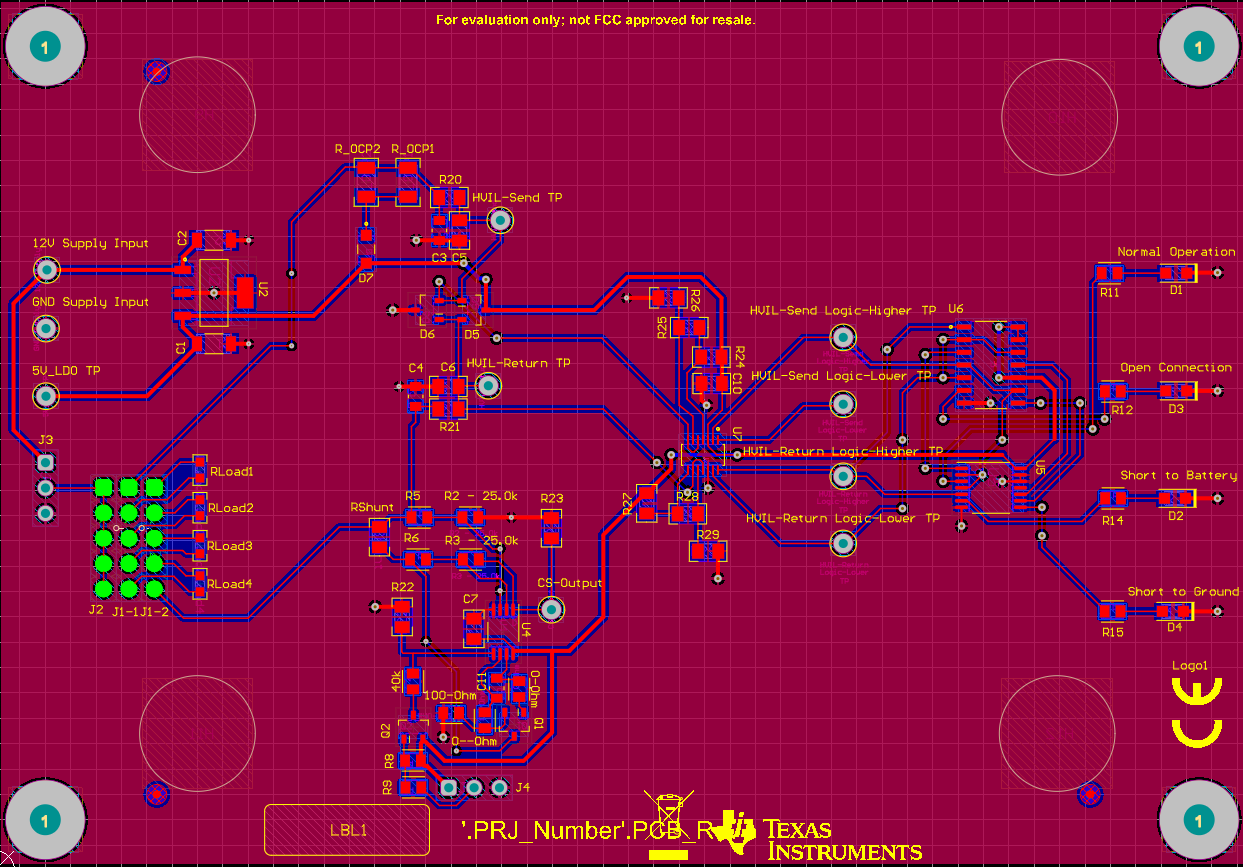
Figure 3-6 shows where different pin headers are located on the PCB. The 1 × 5 pin header columns labeled J1-1 and J1-2 are connected to each endpoint of load resistors: RLoad1, RLoad2, RLoad3, and RLoad4. Connecting all five rows of J1-1 to J1-2 together with 2-pin PCB shunt connectors creates a series connection between all four load resistors. This is the connection used for the Normal Operation condition. Disconnecting any 2-pin PCB shunt connectors between J1-1 and J1-2 creates an open connection (disconnect), which is used for the Open Connection condition.
The 1 × 5 pin header column labeled J2 has a short between all pins, causing J2 to behave like a supply voltage bus rail. The 1 × 3 pin header column labeled J3 has row 1 connected to the 12V supply input, row 2 connected to J2, and row 3 connected to ground. When a single 2-pin PCB shunt connector is connected between row 1 and row 2 of J3, J2 becomes a bus rail to the 12V supply voltage. When a single 2-pin PCB shunt connector is connected between row 2 and row 3 of J3, J2 becomes a bus rail to the ground supply voltage. A 3-pin PCB shunt connectors between columns J2, J1-1, and J1-2, inserts a short to either the 12V supply voltage or ground supply to the corresponding row. This short can be inserted either before the four load resistors,in-between any of the resistors, or after the load.
The 3 × 1 pin header row labeled J4 is used to control the shutdown functionality of the board. Column 1 is connected to the 5V voltage through the pullup resistor R8. Column 2 is connected to the base of transistor Q2, which is operating as a switch. Column 3 is connected to the ground supply voltage. When a 2-pin PCB shunt connector is inserted between column 1 and 2, the shutdown functionality is turned on (active high), and the current source enters shutdown mode. When a 2-pin PCB shunt connector is inserted between column 2 and 3, the shutdown functionality is inactive (active low), and the system operates as anticipated.
 Figure 3-6 TIDA-020069 PCB Header
Connections
Figure 3-6 TIDA-020069 PCB Header
ConnectionsDC voltage and current measurements were taken with a digital multimeter at numerous points on the board. The following test points were measured during multiple modes of operation: 5V_LDO TP, HVIL-Send TP, HVIL-Return TP, HVIL-Send Logic-Higher TP, HVIL-Send Logic-Lower TP, HVIL-Return Logic-Higher TP, HVIL-Higher Logic-Lower TP, and CS-Output. The test results are located in the following section, Test Results.