TIDUF77 June 2024 MSPM0G1507
- 1
- Description
- Resources
- Features
- Applications
- 6
- 1System Description
-
2System Overview
- 2.1 Block Diagram
- 2.2 Design Considerations
- 2.3 Highlighted Products
- 2.4
System Design Theory
- 2.4.1
Hardware Design
- 2.4.1.1 Modular Design
- 2.4.1.2 Auxiliary Flyback Power Supply
- 2.4.1.3 DC Link Voltage Sensing
- 2.4.1.4 Inrush Current Protection
- 2.4.1.5 Motor Phase Voltage Sensing
- 2.4.1.6 Motor Phase Current Sensing
- 2.4.1.7 Over Current Protection of DRV7308
- 2.4.1.8 Internal Overcurrent Protection for TMS320F2800F137
- 2.4.2 Three-Phase PMSM Drive
- 2.4.1
Hardware Design
-
3Hardware, Software, Testing Requirements, and Test Results
- 3.1 Getting Started Hardware
- 3.2 Getting Started GUI
- 3.3
Getting Started C2000 Firmware
- 3.3.1 Download and Install Software Required for Board Test
- 3.3.2 Opening Project Inside CCS
- 3.3.3 Project Structure
- 3.3.4 Test Procedure
- 3.4
Test Results
- 3.4.1 Fast and clean Rising/Falling Edge
- 3.4.2 Inrush Current Protection
- 3.4.3 Thermal performance under 300VDC
- 3.4.4 Thermal performance under 220VAC
- 3.4.5 Overcurrent Protection by Internal CMPSS
- 3.4.6 IPM Efficiency with External Bias Supply under 300VDC
- 3.4.7 Board Efficiency with Onboard Bias Supply under 300VDC
- 3.4.8 Board Efficiency with External Bias Supply under 220VAC
- 3.4.9 Board Efficiency with Onboard Bias Supply under 220VAC
- 3.4.10 iTHD Test of Motor Phase Current
- 3.4.11 Standby Power Test
- 3.5 Migrate Firmware to a New Hardware Board
- 3.6 Getting Started MSPM0 Firmware
- 4Design and Documentation Support
- 5About the Author
2.4.2.4.1.2 Single-Shunt Current Sensing
The single-shunt current-sensing technique measures the DC-link bus current, with knowledge of the power FET switching states and reconstructs the three-phase current of the motor. The detailed description of the single shunt technique is described in the Sensorless-FOC for PMSM With Single DC-Link Shunt application note.
On this reference board, implement the single-shunt current-sensing technique by removing two shunts and shorting the connection of the U, V, W ground of the power module as shown in Figure 2-32.
- On the motherboard, remove current shunt resistors R97, and R104, keep only shunt resistor R83 to sense the DC-Link current.
- On TMS320F2800137 daughterboard, remove U9 and related parts and also remove C61 to increase bandwidth of internal amaplifier of DRV7308 for single-shunt sampling.
- On the MSPM0G1507 daughterboard, remove components related with internal OPA of MSPM0G1507 to increase the bandwidth for single-shunt sampling.
- Use a thick wire to connect the NU, NV, and NW pins together.

 Figure 2-32 Single-Shunt Current-Sensing Circuit for TMS320F2800137
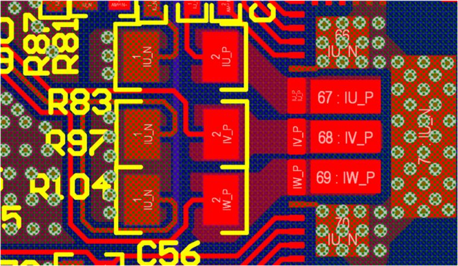
By default, the board has three shunt resistors, Figure 2-33 shows the layout of the shunt resistors. To run with a single-shunt resistor, remove R97 and R104 while keeping R83, solder IW_P, IV_P and IU_P (pin 2 of R83, R97, and R104) together, then all three phase currents flow through only R83.
 Figure 2-33 Shunt Resistors Layout
The DC-Link current is a unidirectional signal, so the DC current offset can be set to a minimum or maximum value to improve the ADC sampling range for the DC-Link current as Figure 2-34 shows. For both daughterboards, change R79 from 20kΩ to 2.2kΩ/1% resistor for the reference voltage to have 0.327V offset for DC current sensing.
 Figure 2-34 DC Offset Reference for Single Shunt of TMS320F2800137 and MSPM0 Daughterboard
The transfer function of this current sampling circuit and the calculation for single shunt are the same as the three shunts.