TIDUFB1 December 2024
- 1
- Description
- Resources
- Features
- Applications
- 6
- 1System Description
-
2System Overview
- 2.1 Block Diagram
- 2.2 Design Considerations
- 2.3 Highlighted Products
- 2.4
Hardware Design
- 2.4.1 Inductor Design
- 2.4.2 Bus Capacitor Selection
- 2.4.3 Input AC Voltage Sensing
- 2.4.4 Output DCBUS Voltage Sensing
- 2.4.5 Auxiliary Power Supply
- 2.4.6 Isolated Power Supply
- 2.4.7 Inductor Current Sensing
- 2.4.8 Gate Driver
- 2.4.9 Isolated Temperature Sensing
- 2.4.10 Overcurrent, Overvoltage Protection (CMPSS)
-
3Hardware, Software, Testing Requirements, and Test Results
- 3.1 Hardware Requirements
- 3.2
Software Requirements
- 3.2.1 Getting Started GUI
- 3.2.2
Getting Started Firmware
- 3.2.2.1 Opening the Project Inside Code Composer Studio™
- 3.2.2.2 Project Structure
- 3.2.2.3 Test Setup
- 3.2.2.4 Running Project
- 3.3
Test Results
- 3.3.1 IGBT Gate Rising and Falling Time
- 3.3.2 Power On Sequence
- 3.3.3 PFC Started by GUI
- 3.3.4 Zero Crossing Under 380VAC, 9kW
- 3.3.5 Current Ripple Under 380VAC,10kW
- 3.3.6 10kW Load Test With Grid Power
- 3.3.7 9kW Load Test With AC Power Source
- 3.3.8 Power Analyzer Results
- 3.3.9 Thermal Performance
- 3.3.10 Voltage Short Interrupt Test
- 3.3.11 Efficiency, iTHD, and Power Factor Results
- 4Design and Documentation Support
- 5About the Author
3.2.2.4.2.1 Running Code (Build 2)
- Run the project by clicking the
 button.
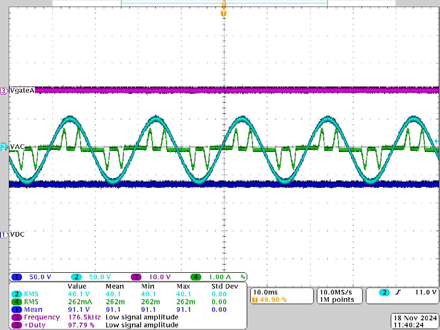
 - Test first at a low voltage. Therefore, the input AC voltage is raised to only 40VRMS, 50Hz.
- Figure 3-17 illustrates the input current and voltage waveform.
 Figure 3-17 Build Level 2: Scope Capture Ia and Va (40VRMS L-N) With PWM Tripped
- CH1 (Blue): DCBUS output voltage
- CH2 (Light blue): AC input phase A voltage
- CH3 (Pink): IGBT gate voltage
- CH4 (Green): AC Input phase A current
- A current reference is set by changing the
iLRefvariable in the Expressions view. This variable is set to 0.02. - Clear the trip by setting the
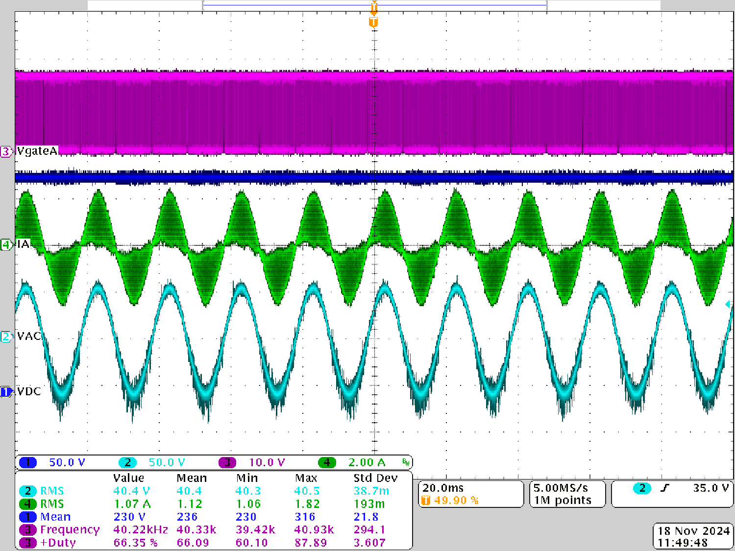
clearTripvariable to 1. - As soon as the trip is cleared, a sinusoidal current
drawn from the input, which verifies correct operation of the current loop.
Figure 3-18 shows the waveform.
 Figure 3-18 Build Level 2: Scope Capture Ia and Va (40VRMS L-N) With
- CH1 (Blue): DCBUS output voltage
- CH2 (Light blue): AC input phase A voltage
- CH3 (Pink): IGBT gate voltage
- CH4 (Green): AC Input phase A current
iLRef= 0.02 - The
guiVbusvariable is close to 230V, and the input AC current per phase is close to 1.07A. - Raise the input AC voltage slowly to 120VRMS. The board maintains
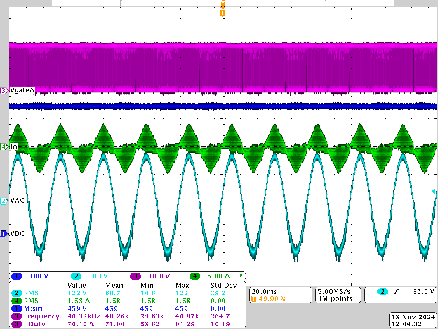
the input current to be constant as the input voltage rises. The output voltage
is raised to 460V. Figure 3-19 shows what the waveforms look like.
 Figure 3-19 Build Level 2: Scope Capture Ia and Va (120VRMS L-N) With
- CH1 (Blue): DCBUS output voltage
- CH2 (Light blue): AC input phase A voltage
- CH3 (Pink): IGBT gate voltage
- CH4 (Green): AC Input phase A current
iLRef= 0.02 - Now raise the current
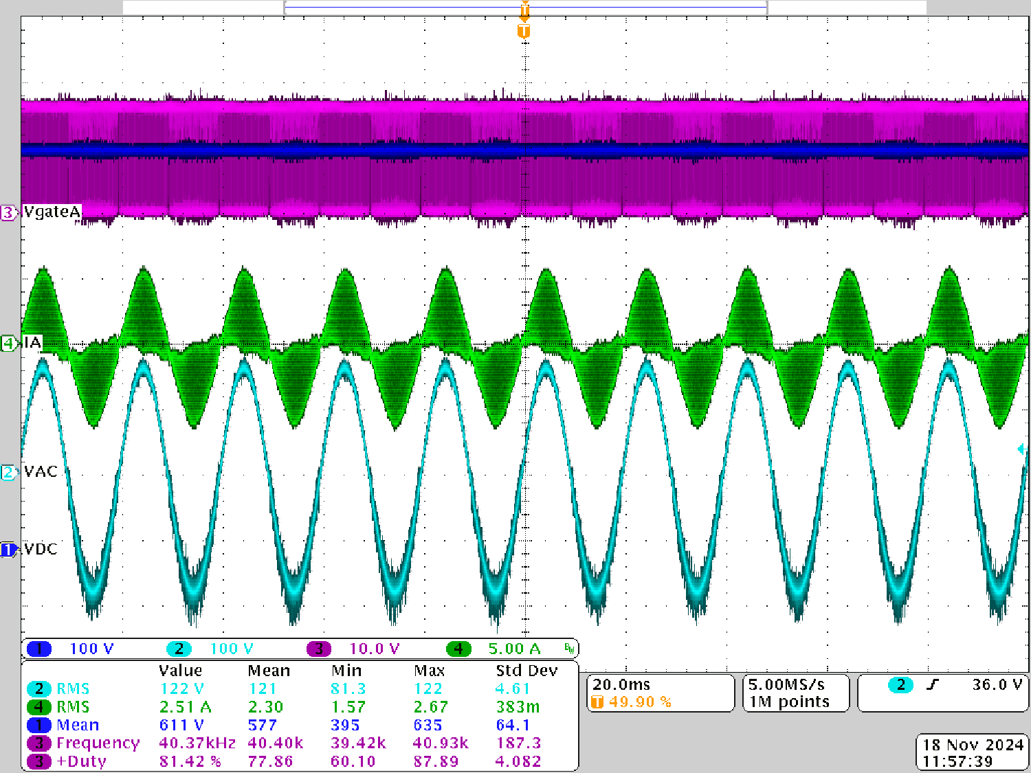
reference
iLRefto 0.05. Observe the bus voltage go to 610V and the input current to around 2.5A. Figure 3-20 shows the waveforms. Figure 3-20 Build Level 2: Scope Capture Ia and Va (120VRMS L-N) With
- CH1 (Blue): DCBUS output voltage
- CH2 (Light blue): AC input phase A voltage
- CH3 (Pink): IGBT gate voltage
- CH4 (Green): AC Input phase A current
iLRef= 0.05 - As only a proportional gain is used in the compensator, the current reference minus the feedback error is never zero. Notice the current drawn deviates slightly from the reference.
- To bring the system to a safe stop, bring the input AC voltage down to zero,
and observe that
guiVBuscomes down to zero as well. - Fully halting the MCU when in real-time mode is a two-step process. First halt the
processor by using the Halt button on the toolbar (
 ) or by using
Target > Halt. Next take the MCU out of real-time mode by
clicking on the
  button. Finally, reset the MCU (
 ) .
) . - Close the CCS debug session by clicking on Terminate Debug Session (Target >
Terminate all).
