TIDUFB1 December 2024
- 1
- Description
- Resources
- Features
- Applications
- 6
- 1System Description
-
2System Overview
- 2.1 Block Diagram
- 2.2 Design Considerations
- 2.3 Highlighted Products
- 2.4
Hardware Design
- 2.4.1 Inductor Design
- 2.4.2 Bus Capacitor Selection
- 2.4.3 Input AC Voltage Sensing
- 2.4.4 Output DCBUS Voltage Sensing
- 2.4.5 Auxiliary Power Supply
- 2.4.6 Isolated Power Supply
- 2.4.7 Inductor Current Sensing
- 2.4.8 Gate Driver
- 2.4.9 Isolated Temperature Sensing
- 2.4.10 Overcurrent, Overvoltage Protection (CMPSS)
-
3Hardware, Software, Testing Requirements, and Test Results
- 3.1 Hardware Requirements
- 3.2
Software Requirements
- 3.2.1 Getting Started GUI
- 3.2.2
Getting Started Firmware
- 3.2.2.1 Opening the Project Inside Code Composer Studio™
- 3.2.2.2 Project Structure
- 3.2.2.3 Test Setup
- 3.2.2.4 Running Project
- 3.3
Test Results
- 3.3.1 IGBT Gate Rising and Falling Time
- 3.3.2 Power On Sequence
- 3.3.3 PFC Started by GUI
- 3.3.4 Zero Crossing Under 380VAC, 9kW
- 3.3.5 Current Ripple Under 380VAC,10kW
- 3.3.6 10kW Load Test With Grid Power
- 3.3.7 9kW Load Test With AC Power Source
- 3.3.8 Power Analyzer Results
- 3.3.9 Thermal Performance
- 3.3.10 Voltage Short Interrupt Test
- 3.3.11 Efficiency, iTHD, and Power Factor Results
- 4Design and Documentation Support
- 5About the Author
2.2.1.3 DC Bus Regulation Loop
The DC bus regulation loop is assumed to be providing the power reference. This loop is divided by the square of the line voltages RMS to provide the conductance, which is further multiplied by the line voltage to give the instantaneous current command.
A small signal model of the DC bus regulation loop is developed by linearizing Equation 3 around the operating point.
For resistive load, the bus voltage and current relate as shown in Equation 4.
The DC voltage regulation loop control model can be drawn, as shown in Figure 2-5. An additional Vbus feedforward is applied to make the control loop independent of the bus voltage, and, thus, the plant model for the bus control can be written as shown in Equation 5.
where
- Hp_bus is the voltage loop plant as seen by the digital controller Gv.
- Output of the Gv is the power reference Po*
- vbus* is the voltage command and voltage reference, vbus is the actual bus voltage.
- Co is the output capacitor, RL is the load resistance.
Using Figure 2-5, a proportional integrator (PI) compensator is designed for the voltage loop. The bandwidth of this loop is kept low as the loop is in conflict with the THD below steady state.
 Figure 2-5 DC Voltage Loop Control
Model
Figure 2-5 DC Voltage Loop Control
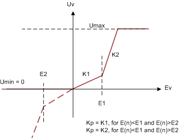
ModelAdditionally, a non-linear PI loop is used to reduce the transients in case of step load changes. Figure 2-6 shows the structure of the non-linear PI loop implemented on this design
 Figure 2-6 Non-Linear PI Loop for Voltage
Controller