TIDUFB1 December 2024
- 1
- Description
- Resources
- Features
- Applications
- 6
- 1System Description
-
2System Overview
- 2.1 Block Diagram
- 2.2 Design Considerations
- 2.3 Highlighted Products
- 2.4
Hardware Design
- 2.4.1 Inductor Design
- 2.4.2 Bus Capacitor Selection
- 2.4.3 Input AC Voltage Sensing
- 2.4.4 Output DCBUS Voltage Sensing
- 2.4.5 Auxiliary Power Supply
- 2.4.6 Isolated Power Supply
- 2.4.7 Inductor Current Sensing
- 2.4.8 Gate Driver
- 2.4.9 Isolated Temperature Sensing
- 2.4.10 Overcurrent, Overvoltage Protection (CMPSS)
-
3Hardware, Software, Testing Requirements, and Test Results
- 3.1 Hardware Requirements
- 3.2
Software Requirements
- 3.2.1 Getting Started GUI
- 3.2.2
Getting Started Firmware
- 3.2.2.1 Opening the Project Inside Code Composer Studio™
- 3.2.2.2 Project Structure
- 3.2.2.3 Test Setup
- 3.2.2.4 Running Project
- 3.3
Test Results
- 3.3.1 IGBT Gate Rising and Falling Time
- 3.3.2 Power On Sequence
- 3.3.3 PFC Started by GUI
- 3.3.4 Zero Crossing Under 380VAC, 9kW
- 3.3.5 Current Ripple Under 380VAC,10kW
- 3.3.6 10kW Load Test With Grid Power
- 3.3.7 9kW Load Test With AC Power Source
- 3.3.8 Power Analyzer Results
- 3.3.9 Thermal Performance
- 3.3.10 Voltage Short Interrupt Test
- 3.3.11 Efficiency, iTHD, and Power Factor Results
- 4Design and Documentation Support
- 5About the Author
2.2.1.1 PWM Modulation
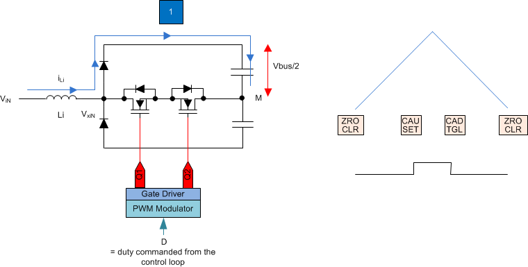
Figure 2-2 shows a simplified, single-phase diagram of the Vienna rectifier. To control this rectifier, the duty cycle is controlled to regulate the voltage vxiN directly. That is, if the software variable Duty is set to 1, vxiN becomes the highest voltage possible by never turning the Q1 and Q2 switches on and letting the inductor connect to the DC bus though the bridge diode. Similarly when Duty is set to 0, PWM is modulated such that Q1 and Q2 always conduct, making vxiN connect to the midpoint of the DC bus (which is zero), which creates the lowest possible voltage for the switching cycle.
 Figure 2-2 Single Phase Diagram of Vienna Rectifier
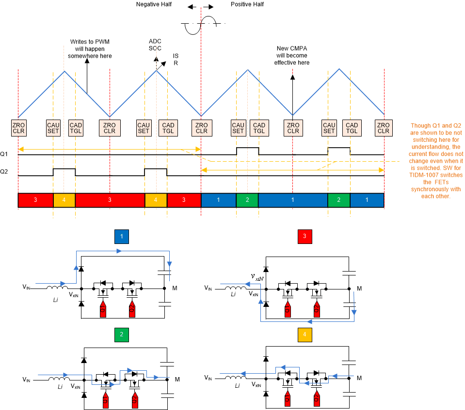
Figure 2-3 shows the detailed PWM configuration.
 Figure 2-3 Vienna Rectifier Detailed PWM Modulation Scheme