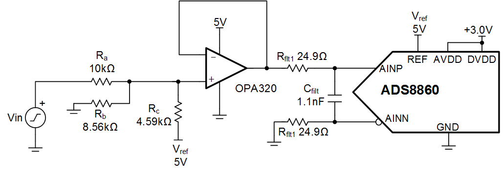
Noninverting Circuit for High-to-Low Voltage Level Translation To Drive ADC
| Input | ADC Input | Digital Output ADS8860 |
|---|---|---|
| –10V | 0.2V | 0A3DH or 2621d |
| 10V | 4.8V | F5C3H or 62915d |
| Vref | AVDD | DVDD |
|---|---|---|
| 5V | 3.0V | 3.0V |
Design Description
This circuit document describes how to translate a high-voltage signal (for example, ±10V) to a low voltage ADC input (for example, 0V to 5V). This circuit does not require any high-voltage supply to operate, but rather uses a voltage divider and level shift to translate the input signal. This circuit shows the OPA320 op amp and ADS8860 SAR ADC, but the topology applies to many different ADCs. This design can be used in a wide range of applications where a high-voltage input needs to be translated such as analog input modules for PLCs, analytical lab instrumentation, and factory automation and control.
Specifications
| Specification | Goal | Calculated | Simulated |
|---|---|---|---|
| Bandwidth | > 1MHz | 2.9MHz | 4.06MHz |
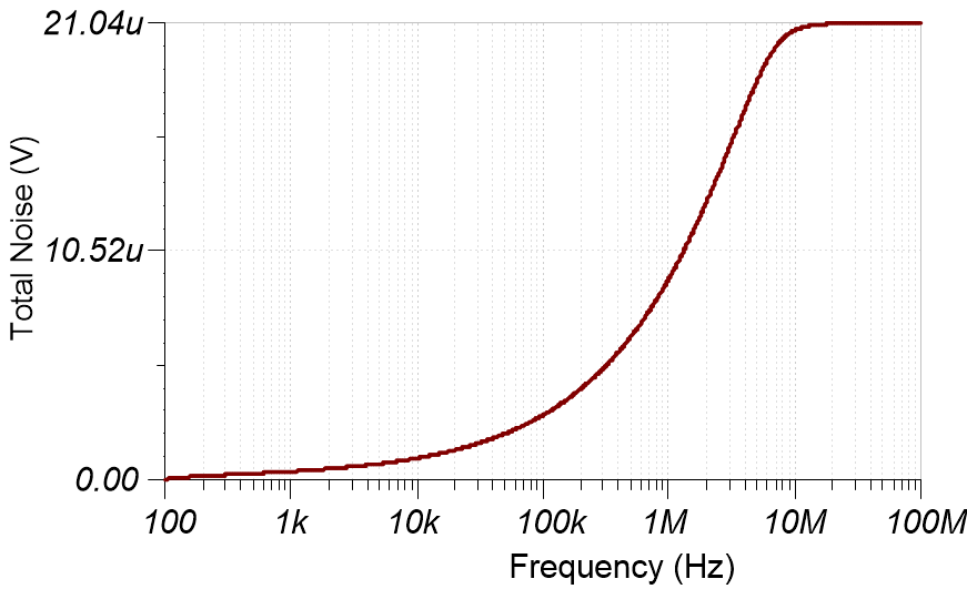
| Noise | < 1/2LSB = 38.1µV | 23.56µVRMS | 21.04NµVRMS |
| Transient settling error | < 1/2 LSB = 38.1µV | 35µV |
Design Notes
- Select a C0G type capacitor for Cfilt to minimize distortion.
- Use 0.1% 20ppm/°C film resistors or better to minimize gain error and drift.
- The input impedance of this circuit is Rin = Ra + Rb||Rc. For a high-impedance input, use a high-voltage amplifier buffer (for example, Vcc = +15V and Vee = –15V). Alternatively, increase the input impedance by multiplying Ra, Rb, and Rc by the same factor. However, increasing the resistance on all the resistors impacts the system noise.
Component Selection
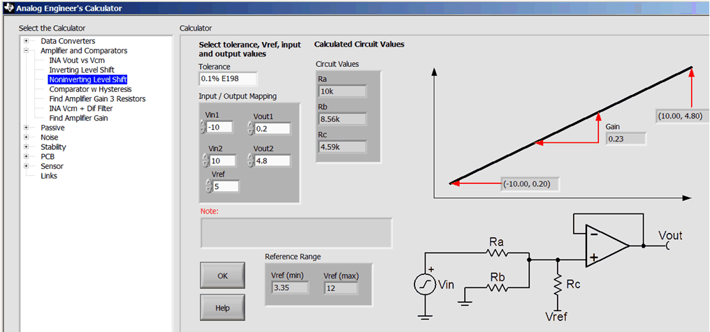
- The first step is to select the amplifier input and output range. In this example, the input range is –10V to +10V. The amplifier output range is set according to the ADC input and the amplifier linear output range. The ADC input range in this example is set by the reference voltage and is 5V. The amplifier supply is set to 5V to match the ADC input range. The output of the amplifier cannot swing to the power supply rails because of output swing limitations (that is, linear range for OPA320 0.1V < VOUT < 4.9V). For this example, an output swing of 0.2V to 4.8V is selected for the input signal of –10V to 10V. The output range could have been set as 0.1V to 4.9V to match the linear range, but in this example design margin is added to account for power supply variation.
- Use the Analog Engineer's Calculator in the next step to select
component values. Enter the input and output voltages and reference voltage
(–10V < VIN < +10V, and 0.2V < VOUT < 4.8V).
The range of acceptable reference voltages is given at the bottom of the tool
(3.35V to 12V, in this example). A reference of 5V is selected as this reference
voltage is available elsewhere in the circuit. The tool outputs the 0.1%
resistors required to map the voltages (Ra = 10kΩ, Rb =
8.56kΩ, Rc = 4.59kΩ).
- The following equations show the
transfer function for the non-inverting level-shift topology. It is possible to
use these equations to solve for the different component values rather than the
calculator. To do this, choose a reference value and fix the value of
Ra to 10kΩ. Once this is done, solve for Rb and
Rc for two different values of output signal. The algebra for
this problem is a little complex, so the calculator is the suggested method. Use
the equations to verify the transfer function as the equation following shows.
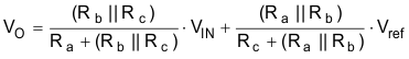
where
-
Using the values from the calculator:
Ra = 10kΩ, Rb = 8.56kΩ, Rc = 4.59kΩVO = 0.23005V × VIN + 2.506VVO(–10V) = 0.2055VVO(+10V) = 4.8065V
-
- Find Rfilt and Cfilt to allow for settling at 1Msps. The Refine the Rfilt and Cfilt Values on ADC drive video from the TI Precision Labs - ADCs video series shows the algorithm for selecting Rfilt and Cfilt. The final value of 24.9Ω and 1.1nF proved to settle to well below ½ of a least significant bit (LSB).
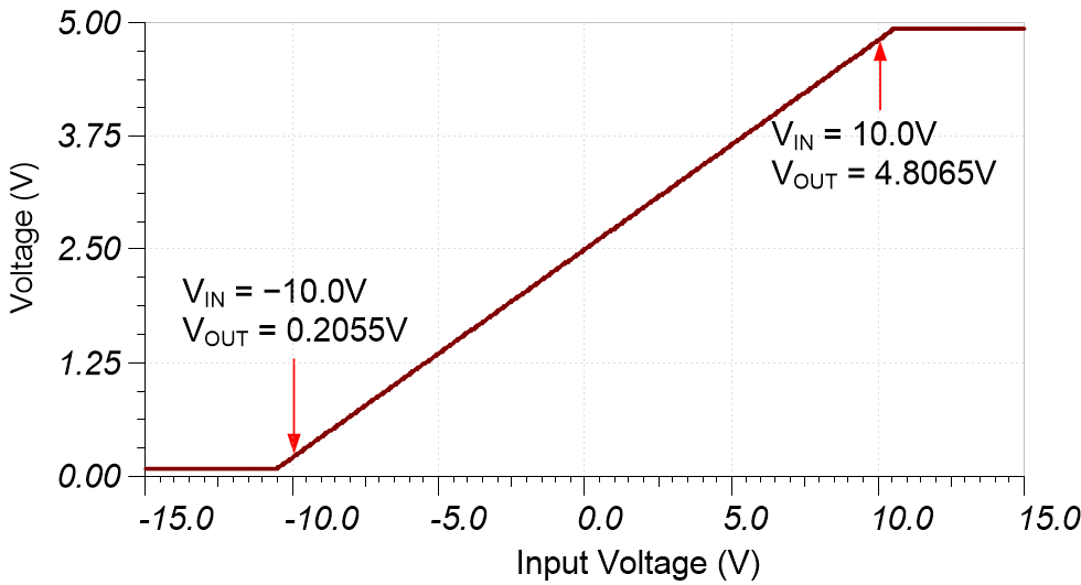
DC Transfer Characteristics
The following graph shows the linear output response for a –10V to 10V input. In this case, the amplifier output is approximately 0.2V for a –10V input and 4.8V for a +10V input. This design was scaled so that the output range avoids the nonlinear power supply rails by 0.2V. See the TI Precision Labs - ADCs Determining a SAR ADC's Linear Range when using operational amplifiers video for detailed theory on this subject.
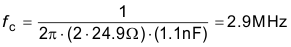
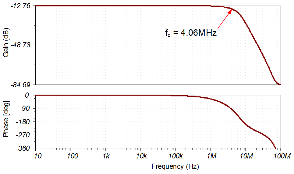
AC Transfer Characteristics
The bandwidth is limited by the RC charge bucket circuit. The calculated and simulated bandwidth compare well (calculated fc = 2.9MHz, simulated fc = 4.06MHz). The small discrepancy in the bandwidth is due to gain peaking on the OPA320 device.
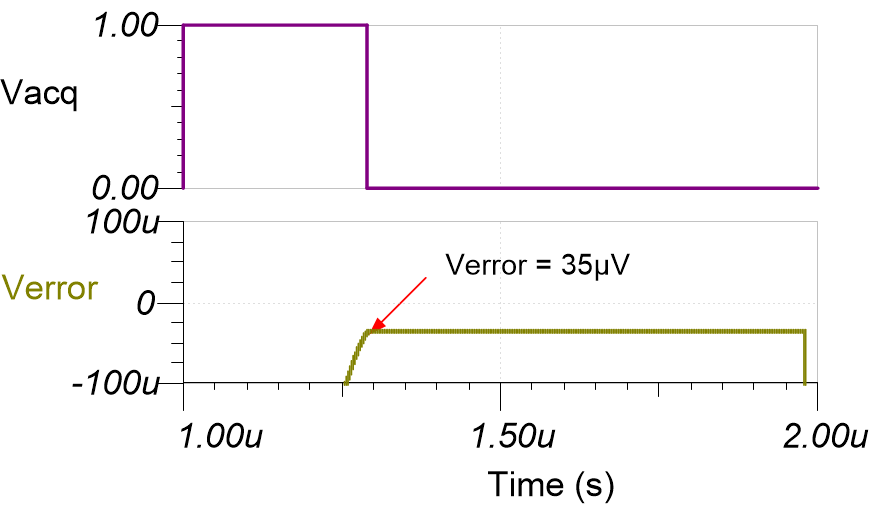
Transient ADC Input Settling Simulation
The following simulation shows settling to a +10-V DC input signal. This type of simulation shows that the sample and hold kickback circuit is properly selected. See the Final SAR ADC Drive Simulations video for detailed theory on this subject.
Noise Simulation
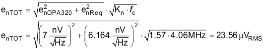
The following noise calculation takes into account the thermal noise of the resistor network, the amplifier noise, and the bandwidth limit from the RC filter. The calculated total noise is 23.5µVRMS and the simulated total noise is 21.04µVRMS. See the Op Amp Noise Calculation video for detailed theory on amplifier noise calculations, and the Calculating the total noise for ADC Systems video for data converter noise.
Noise equivalent input resistor network:
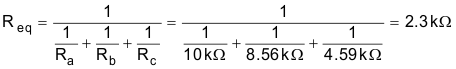
Resistor network noise:

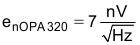
OPS320 noise density:
Total noise:
Design Featured Devices and Alternative Parts
| Device | Key Features | Link | Other Possible Devices |
|---|---|---|---|
| ADS8860 | 16-bit resolution, SPI, 1-Msps sample rate, single-ended input, Vref input range 2.5V to 5.0V | 16-bit, 1MSPS, 1-channel SAR ADC with single-ended input, SPI and daisy chain | Precision ADCs |
| OPA320 | 20-MHz bandwidth, rail-to-rail with zero crossover distortion, VOS(MAX) = 150μV, VOS(DriftMAX) = 5μV/°C, en = 7nV/√ Hz | Precision, zero-crossover, 20MHz, 0.9pA Ib, RRIO, CMOS operational amplifier | Operational amplifiers (op amps) |
Link to Key Files
Texas Instruments, SBAC250 sources files, software support
Trademarks
All trademarks are the property of their respective owners.
IMPORTANT NOTICE AND DISCLAIMER
TI PROVIDES TECHNICAL AND RELIABILITY DATA (INCLUDING DATASHEETS), DESIGN RESOURCES (INCLUDING REFERENCE DESIGNS), APPLICATION OR OTHER DESIGN ADVICE, WEB TOOLS, SAFETY INFORMATION, AND OTHER RESOURCES “AS IS” AND WITH ALL FAULTS, AND DISCLAIMS ALL WARRANTIES, EXPRESS AND IMPLIED, INCLUDING WITHOUT LIMITATION ANY IMPLIED WARRANTIES OF MERCHANTABILITY, FITNESS FOR A PARTICULAR PURPOSE OR NON-INFRINGEMENT OF THIRD PARTY INTELLECTUAL PROPERTY RIGHTS.
These resources are intended for skilled developers designing with TI products. You are solely responsible for (1) selecting the appropriate TI products for your application, (2) designing, validating and testing your application, and (3) ensuring your application meets applicable standards, and any other safety, security, or other requirements. These resources are subject to change without notice. TI grants you permission to use these resources only for development of an application that uses the TI products described in the resource. Other reproduction and display of these resources is prohibited. No license is granted to any other TI intellectual property right or to any third party intellectual property right. TI disclaims responsibility for, and you will fully indemnify TI and its representatives against, any claims, damages, costs, losses, and liabilities arising out of your use of these resources.
TI’s products are provided subject to TI’s Terms of Sale (www.ti.com/legal/termsofsale.html) or other applicable terms available either on ti.com or provided in conjunction with such TI products. TI’s provision of these resources does not expand or otherwise alter TI’s applicable warranties or warranty disclaimers for TI products.
Mailing Address: Texas Instruments, Post Office Box 655303, Dallas, Texas 75265
Copyright © 2024, Texas Instruments Incorporated