-
ADS4249 Dual-Channel, 14-Bit, 250-MSPS Ultralow-Power ADC
- 1 Features
- 2 Applications
- 3 Description
- 4 Revision History
- 5 ADS424x, ADS422x Family Comparison
- 6 Pin Configuration and Functions
-
7 Specifications
- 7.1 Absolute Maximum Ratings
- 7.2 ESD Ratings
- 7.3 Recommended Operating Conditions
- 7.4 Thermal Information
- 7.5 Electrical Characteristics: ADS4249 (250 MSPS)
- 7.6 Electrical Characteristics: General
- 7.7 Digital Characteristics
- 7.8 LVDS and CMOS Modes Timing Requirements
- 7.9 LVDS Timings at Lower Sampling Frequencies
- 7.10 CMOS Timings at Lower Sampling Frequencies
- 7.11 Serial Interface Timing Characteristics
- 7.12 Reset Timing (Only when Serial Interface is Used)
- 7.13 Typical Characteristics
-
8 Detailed Description
- 8.1 Overview
- 8.2 Functional Block Diagram
- 8.3 Feature Description
- 8.4 Device Functional Modes
- 8.5 Programming
- 8.6
Register Maps
- 8.6.1 Serial Register Map
- 8.6.2
Description of Serial Registers
- 8.6.2.1 Register Address 00h (Default = 00h)
- 8.6.2.2 Register Address 01h (Default = 00h)
- 8.6.2.3 Register Address 01h (Default = 00h)
- 8.6.2.4 Register Address 25h (Default = 00h)
- 8.6.2.5 Register Address 29h (Default = 00h)
- 8.6.2.6 Register Address 2Bh (Default = 00h)
- 8.6.2.7 Register Address 3Dh (Default = 00h)
- 8.6.2.8 Register Address 3Fh (Default = 00h)
- 8.6.2.9 Register Address 40h (Default = 00h)
- 8.6.2.10 Register Address 41h (Default = 00h)
- 8.6.2.11 Register Address 42h (Default = 00h)
- 8.6.2.12 Register Address 45h (Default = 00h)
- 8.6.2.13 Register Address 4Ah (Default = 00h)
- 8.6.2.14 Register Address 58h (Default = 00h)
- 8.6.2.15 Register Address BFh (Default = 00h)
- 8.6.2.16 Register Address C1h (Default = 00h)
- 8.6.2.17 Register Address CFh (Default = 00h)
- 8.6.2.18 Register Address EFh (Default = 00h)
- 8.6.2.19 Register Address F1h (Default = 00h)
- 8.6.2.20 Register Address F2h (Default = 00h)
- 8.6.2.21 Register Address 2h (Default = 00h)
- 8.6.2.22 Register Address D5h (Default = 00h)
- 8.6.2.23 Register Address D7h (Default = 00h)
- 8.6.2.24 Register Address DBh (Default = 00h)
- 9 Application and Implementation
- 10Power Supply Recommendations
- 11Layout
- 12Device and Documentation Support
- 13Mechanical, Packaging, and Orderable Information
- IMPORTANT NOTICE
ADS4249 Dual-Channel, 14-Bit, 250-MSPS Ultralow-Power ADC
1 Features
- Maximum Sample Rate: 250 MSPS
- Ultra-Low Power with Single 1.8-V Supply:
- 560-mW Total Power at 250 MSPS
- High Dynamic Performance:
- 80-dBc SFDR at 170 MHz
- 71.7-dBFS SNR at 170 MHz
- Crosstalk: > 90 dB at 185 MHz
- Programmable Gain up to 6 dB for
SNR/SFDR Trade-off - DC Offset Correction
- Output Interface Options:
- 1.8-V Parallel CMOS Interface
- Double Data Rate (DDR) LVDS with Programmable Swing:
- Standard Swing: 350 mV
- Low Swing: 200 mV
- Supports Low Input Clock Amplitude
Down to 200 mVPP - Package: 9-mm × 9-mm, 64-Pin VQFN Package
2 Applications
- Wireless Communications Infrastructure
- Software Defined Radios
- Power Amplifier Linearization
3 Description
The ADS4249 is a member of the ADS42xx ultralow-power family of dual-channel, 12-bit and 14-bit analog-to-digital converters (ADCs). Innovative design techniques are used to achieve high dynamic performance and consume extremely low power with a 1.8-V supply. This topology makes the ADS4249 well-suited for multi-carrier, wide-bandwidth communications applications.
The ADS4249 has gain options that can be used to improve SFDR performance at lower full-scale input ranges. This device also includes a dc offset correction loop that can be used to cancel the ADC offset. Both DDR LVDS and parallel CMOS digital output interfaces are available in a compact VQFN-64 PowerPAD™ package.
The device includes internal references and the traditional reference pins and associated decoupling capacitors have been eliminated. The ADS4249 is specified over the industrial temperature range (–40°C to 85°C).
Device Information(1)
| PART NUMBER | PACKAGE | BODY SIZE (NOM) |
|---|---|---|
| ADS4249 | VQFN (64) | 9.00 mm × 9.00 mm |
- For all available packages, see the orderable addendum at the end of the data sheet.
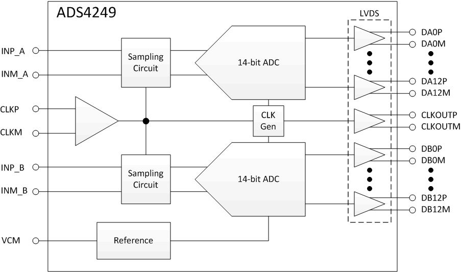
ADS4249 Block Diagram

4 Revision History
Changes from D Revision (May 2015) to E Revision
- Changed Pin Functions (LVDS Mode) table to comply with RGC Package (LVDS Mode) pin out diagramGo
- Changed Pin Functions (CMOS Mode) table to comply with RGC Package (CMOS Mode) pin out diagram Go
- Changed unit in last row of Clock Input, Input clock amplitude differential parameter to VPP in Recommended Operating Conditions tableGo
- Added text reference for Table 5 Go
Changes from C Revision (July 2012) to D Revision
- Added Pin Configuration and Functions section, ESD Ratings table, Feature Description section, Device Functional Modes, Application and Implementation section, Power Supply Recommendations section, Layout section, Device and Documentation Support section, and Mechanical, Packaging, and Orderable Information section Go
Changes from B Revision (September 2011) to C Revision
- Changed footnote 1 in CMOS Timings at Lower Sampling FrequenciesGo
- Changed conditions for ADS4249 Typical Characteristics sectionGo
- Changed register D5h bit names of bits D7, D4, D3, and D0 in Table 10Go
- Changed register address D8 to DB in Table 10Go
- Changed register address D5h to match change in Table 10Go
- Changed register address DB to match change in Table 10Go
Changes from A Revision (September 2011) to B Revision
5 ADS424x, ADS422x Family Comparison(1)
| 65 MSPS | 125 MSPS | 160 MSPS | 250 MSPS | |
|---|---|---|---|---|
| ADS422x 12-bit family |
ADS4222 | ADS4225 | ADS4226 | ADS4229 |
| ADS424x 14-bit family |
ADS4242 | ADS4245 | ADS4246 | ADS4249 |
The ADS4249 is pin-compatible with the previous generation ADS62P49 data converter; this similar architecture enables easy migration. However, there are some important differences between the two device generations, summarized in Table 1.
Table 1. Migrating from the ADS62P49
| ADS62P49 | ADS4249 |
|---|---|
| PINS | |
| Pin 22 is NC (not connected) | Pin 22 is AVDD |
| Pins 38 and 58 are DRVDD | Pins 38 and 58 are NC (do not connect, must be floated) |
| Pins 39 and 59 are DRGND | Pins 39 and 59 are NC (do not connect, must be floated) |
| SUPPLY | |
| AVDD is 3.3 V | AVDD is 1.8 V |
| DRVDD is 1.8 V | No change |
| INPUT COMMON-MODE VOLTAGE | |
| VCM is 1.5 V | VCM is 0.95 V |
| SERIAL INTERFACE | |
| Protocol: 8-bit register address and 8-bit register data | No change in protocol New serial register map |
| EXTERNAL REFERENCE | |
| Supported | Not supported |
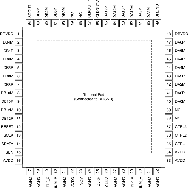
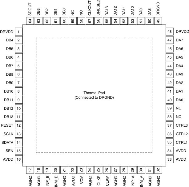
6 Pin Configuration and Functions

NOTE:
The PowerPAD is connected to DRGND.Pin Functions (LVDS Mode)
| PIN | I/O | DESCRIPTION | |
|---|---|---|---|
| NAME | NO. | ||
| AGND | 17 | I | Analog ground |
| 18 | |||
| 21 | |||
| 24 | |||
| 27 | |||
| 28 | |||
| 31 | |||
| 32 | |||
| AVDD | 16 | I | Analog power supply |
| 22 | |||
| 33 | |||
| 34 | |||
| CLKM | 26 | I | Differential clock negative input |
| CLKP | 25 | I | Differential clock positive input |
| CLKOUTP | 57 | O | Differential output clock, true |
| CLKOUTM | 56 | O | Differential output clock, complement |
| CTRL1 | 35 | I | Digital control input pins. Together, these pins control the various power-down modes. |
| CTRL2 | 36 | ||
| CTRL3 | 37 | ||
| DA0M | 40 | O | Channel A differential output data pair, D0 and D1 multiplexed |
| DA0P | 41 | ||
| DA2M | 42 | O | Channel A differential output data D2 and D3 multiplexed |
| DA2P | 43 | ||
| DA4M | 44 | O | Channel A differential output data D4 and D5 multiplexed |
| DA4P | 45 | ||
| DA6M | 46 | O | Channel A differential output data D6 and D7 multiplexed |
| DA6P | 47 | ||
| DA8M | 50 | O | Channel A differential output data D8 and D9 multiplexed |
| DA8P | 51 | ||
| DA10M | 52 | O | Channel A differential output data D10 and D11 multiplexed |
| DA10P | 53 | ||
| DA12M | 54 | O | Channel A differential output data D12 and D13 multiplexed |
| DA12P | 55 | ||
| DB0M | 60 | O | Channel B differential output data pair, D0 and D1 multiplexed |
| DB0P | 61 | ||
| DB2M | 62 | O | Channel B differential output data D2 and D3 multiplexed |
| DB2P | 63 | ||
| DB4M | 2 | O | Channel B differential output data D4 and D5 multiplexed |
| DB4P | 3 | ||
| DB6M | 4 | O | Channel B differential output data D6 and D7 multiplexed |
| DB6P | 5 | ||
| DB8M | 6 | O | Channel B differential output data D8 and D9 multiplexed |
| DB8P | 7 | ||
| DB10M | 8 | O | Channel B differential output data D10 and D11 multiplexed |
| DB10P | 9 | ||
| DB12M | 10 | O | Channel B differential output data D12 and D13 multiplexed |
| DB12P | 11 | ||
| DRGND | 49 | I | Output buffer ground |
| PAD | |||
| DRVDD | 1 | I | Output buffer supply |
| 48 | |||
| INM_A | 30 | I | Differential analog negative input, channel A |
| INP_A | 29 | I | Differential analog positive input, channel A |
| INM_B | 20 | I | Differential analog negative input, channel B |
| INP_B | 19 | I | Differential analog positive input, channel B |
| NC | 38 | — | Do not connect, must be floated |
| 39 | |||
| 58 | |||
| 59 | |||
| RESET | 12 | I | Serial interface RESET input. When using the serial interface mode, the internal registers must be initialized through a hardware RESET by applying a high pulse on this pin or by using the software reset option; see the Serial Interface Configuration section. In parallel interface mode, the RESET pin must be permanently tied high. SCLK and SEN are used as parallel control pins in this mode. This pin has an internal 150-kΩ pull-down resistor. |
| SCLK | 13 | I | This pin functions as a serial interface clock input when RESET is low. SCLK controls the low-speed mode selection when RESET is tied high; see Table 7 for detailed information. This pin has an internal 150-kΩ pull-down resistor. |
| SDATA | 14 | I | Serial interface data input; this pin has an internal 150-kΩ pull-down resistor. |
| SDOUT | 64 | O | This pin functions as a serial interface register readout when the READOUT bit is enabled. When READOUT = 0, this pin is put into a high-impedance state. |
| SEN | 15 | I | This pin functions as a serial interface enable input when RESET is low. SEN controls the output interface and data format selection when RESET is tied high; see Table 8 for detailed information. This pin has an internal 150-kΩ pull-up resistor to AVDD. |
| VCM | 23 | O | This pin outputs the common-mode voltage (0.95 V) that can be used externally to bias the analog input pins |

NOTE:
The PowerPAD is connected to DRGND.Pin Functions (CMOS Mode)
| PIN | I/O | DESCRIPTION | |
|---|---|---|---|
| NAME | NO. | ||
| AGND | 17 | I | Analog ground |
| 18 | |||
| 21 | |||
| 24 | |||
| 27 | |||
| 28 | |||
| 31 | |||
| 32 | |||
| AVDD | 16 | I | Analog power supply |
| 22 | |||
| 33 | |||
| 34 | |||
| CLKM | 26 | I | Differential clock negative input |
| CLKP | 25 | I | Differential clock positive input |
| CLKOUT | 57 | O | CMOS output clock |
| CTRL1 | 35 | I | Digital control input pins. Together, these pins control various power-down modes. |
| CTRL2 | 36 | ||
| CTRL3 | 37 | ||
| DA0 | 40 | O | Channel A ADC output data bits, CMOS levels |
| DA1 | 41 | ||
| DA2 | 42 | ||
| DA3 | 43 | ||
| DA4 | 44 | ||
| DA5 | 45 | ||
| DA6 | 46 | ||
| DA7 | 47 | ||
| DA8 | 50 | ||
| DA9 | 51 | ||
| DA10 | 52 | ||
| DA11 | 53 | ||
| DA12 | 54 | ||
| DA13 | 55 | ||
| DB0 | 60 | O | Channel B ADC output data bits, CMOS levels |
| DB1 | 61 | ||
| DB2 | 62 | ||
| DB3 | 63 | ||
| DB4 | 2 | ||
| DB5 | 3 | ||
| DB6 | 4 | ||
| DB7 | 5 | ||
| DB8 | 6 | ||
| DB9 | 7 | ||
| DB10 | 8 | ||
| DB11 | 9 | ||
| DB12 | 10 | ||
| DB13 | 11 | ||
| DRGND | 49 | I | Output buffer ground |
| PAD | |||
| DRVDD | 1 | I | Output buffer supply |
| 48 | |||
| INM_A | 30 | I | Differential analog negative input, channel A |
| INP_A | 29 | I | Differential analog positive input, channel A |
| INM_B | 20 | I | Differential analog negative input, channel B |
| INP_B | 19 | I | Differential analog positive input, channel B |
| NC | 38 | — | Do not connect, must be floated |
| 39 | |||
| 58 | |||
| 59 | |||
| RESET | 12 | I | Serial interface RESET input. When using the serial interface mode, the internal registers must be initialized through a hardware RESET by applying a high pulse on this pin or by using the software reset option; see the Serial Interface Configuration section. In parallel interface mode, the RESET pin must be permanently tied high. SDATA and SEN are used as parallel control pins in this mode. This pin has an internal 150-kΩ pull-down resistor. |
| SCLK | 13 | I | This pin functions as a serial interface clock input when RESET is low. SCLK controls the low-speed mode when RESET is tied high; see Table 7 for detailed information. This pin has an internal 150-kΩ pull-down resistor. |
| SDATA | 14 | I | Serial interface data input; this pin has an internal 150-kΩ pull-down resistor. |
| SDOUT | 64 | O | This pin functions as a serial interface register readout when the READOUT bit is enabled. When READOUT = 0, this pin is put into a high-impedance state. |
| SEN | 15 | I | This pin functions as a serial interface enable input when RESET is low. SEN controls the output interface and data format selection when RESET is tied high; see Table 8 for detailed information. This pin has an internal 150-kΩ pull-up resistor to AVDD. |
| UNUSED | 56 | — | This pin is not used in the CMOS interface |
| VCM | 23 | O | This pin outputs the common-mode voltage (0.95 V) that can be used externally to bias the analog input pins |