-
TCAN1472-Q1 and TCAN1472V-Q1Functional Safety FIT Rate, FMD, and Pin FMA
TCAN1472-Q1 and
TCAN1472V-Q1
Functional Safety
FIT Rate, FMD, and Pin FMA
Trademarks
All trademarks are the property of their respective owners.
1 Overview
This document contains information for TCAN1472-Q1 and TCAN1472V-Q1 to aid in a functional safety system design. These devices are controller area network (CAN) signal improvement capable (SIC) transceivers compliant to CiA 601-4 and are available in the SOIC (D), VSON (DRB), and SOT (DDF) packages. Information provided are:
- Functional safety failure in time (FIT) rates of the semiconductor component estimated by the application of industry reliability standards
- Component failure modes and their distribution (FMD) based on the primary function of the device
- Pin failure mode analysis (pin FMA) for the device pins of TCAN1472-Q1 and TCAN1472V-Q1
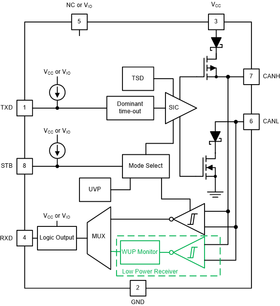
Figure 1-1 shows the device functional block diagram for reference. TCAN1472V-Q1 has the VIO input at pin 5, while TCAN1472-Q1 has a no connect (NC) at pin 5.
 Figure 1-1 TCAN1472-Q1 and
TCAN1472V-Q1 Functional Block Diagram
Figure 1-1 TCAN1472-Q1 and
TCAN1472V-Q1 Functional Block Diagram2 Functional Safety Failure In Time (FIT) Rates
This section provides functional safety failure in time (FIT) rates for TCAN1472-Q1 and TCAN1472V-Q1 based on two different industry-wide used reliability standards:
- Table 2-1 provides FIT rates based on IEC TR 62380 / ISO 26262 part 11
- Table 2-2 provides FIT rates based on the Siemens Norm SN 29500-2
| FIT IEC TR 62380 / ISO 26262 | FIT (Failures Per 109 Hours) 8-pin SOIC (D) | FIT (Failures Per 109 Hours) 8-pin VSON (DRB) | FIT (Failures Per 109 Hours) 8-pin SOT (DDF) |
|---|---|---|---|
| Total component FIT rate | 10 | 7 | 5 |
| Die FIT rate | 3 | 3 | 3 |
| Package FIT rate | 7 | 4 | 2 |
The failure rate and mission profile information in Table 2-1 comes from the reliability data handbook IEC TR 62380 / ISO 26262 part 11:
- Mission profile: Motor control from table 11
- Power dissipation: 132mW
- Climate type: World-wide table 8
- Package factor (lambda 3): Table 17b
- Substrate material: FR4
- EOS FIT rate assumed: 0 FIT
| Table | Category | Reference FIT Rate | Reference Virtual TJ |
|---|---|---|---|
| 5 | CMOS/BICMOS ASICs Analog and Mixed = <50V supply | 25 FIT | 55°C |
The reference FIT rate and reference virtual TJ (junction temperature) in Table 2-2 come from the Siemens Norm SN 29500-2 tables 1 through 5. Failure rates under operating conditions are calculated from the reference failure rate and virtual junction temperature using conversion information in SN 29500-2 section 4.
3 Failure Mode Distribution (FMD)
The failure mode distribution estimation for TCAN1472-Q1 and TCAN1472V-Q1 in Table 3-1 comes from the combination of common failure modes listed in standards such as IEC 61508 and ISO 26262, the ratio of sub-circuit function size and complexity, and from best engineering judgment.
The failure modes listed in this section reflect random failure events and do not include failures resulting from misuse or overstress.
| Die Failure Modes | Failure Mode Distribution (%) |
|---|---|
| Transmitter fail | 52 |
| Receiver fail | 13 |
| Power management or state control fail | 15 |
| Input and output buffer fail | 20 |
4 Pin Failure Mode Analysis (Pin FMA)
This section provides a failure mode analysis (FMA) for the pins of the TCAN1472-Q1 and TCAN1472V-Q1. The failure modes covered in this document include the typical pin-by-pin failure scenarios:
- Pin short-circuited to ground (see Table 4-2)
- Pin open-circuited (see Table 4-3)
- Pin short-circuited to an adjacent pin (see Table 4-4)
- Pin short-circuited to VCC (see Table 4-5)
- Pin short-circuited to VBAT (see Table 4-6)
- Pin short-circuited to VIO (Table 4-7)
Table 4-2 through Table 4-7 also indicate how these pin conditions can affect the device as per the failure effects classification in Table 4-1.
| Class | Failure Effects |
|---|---|
| A | Potential device damage that affects functionality. |
| B | No device damage, but loss of functionality. |
| C | No device damage, but performance degradation. |
| D | No device damage, no impact to functionality or performance. |
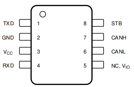
Figure 4-1 shows the TCAN1472-Q1 and TCAN1472V-Q1 SOIC (D) pin diagram.
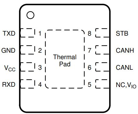
Figure 4-2 shows the TCAN1472-Q1 and TCAN1472V-Q1 VSON (DRB) pin diagram.
Figure 4-3 shows the TCAN1472-Q1 and TCAN1472V-Q1 SOT (DDF) pin diagram.
For a detailed description of the device pins please refer to the Pin Configuration and Functions section in the TCAN1472-Q1 and TCAN1472V-Q1 data sheets.
 Figure 4-1 SOIC (D) Pin Diagram
 Figure 4-3 SOT (DDF) Pin Diagram
 Figure 4-2 VSON
(DRB) Pin Diagram
Figure 4-2 VSON
(DRB) Pin DiagramFollowing are the assumptions of use and the device configuration assumed for the pin FMA in this section:
- VCC = 4.5V to 5.5V
- VBAT = 6V to 24V
- VIO = 1.7V to 5.5V
| Pin Name | Pin No. | Description of Potential Failure Effects | Failure Effect Class |
|---|---|---|---|
| TXD | 1 | Device enters dominant time out mode. Unable to transmit data. | B |
| GND | 2 | None. | D |
| VCC | 3 | Device not powered, high ICC current. | B |
| RXD | 4 | RXD default is high-side FET ON, with pin short-to-ground, forms direct path between supply and ground causing high current. | A |
| NC | 5 | None. | D |
| VIO | 5 | Device is in protected mode. Transceiver is passive on bus. | B |
| CANL | 6 | VO(REC) specification violated. Degraded EMC performance. | C |
| CANH | 7 | Device cannot drive dominant to the bus, no communication is possible. | B |
| STB | 8 | STB stuck low, transceiver unable to enter low-power mode. | B |
| Thermal Pad | - | None. | D |
| Pin Name | Pin No. | Description of Potential Failure Effects | Failure Effect Class |
|---|---|---|---|
| TXD | 1 | TXD pin defaults high, device always recessive and unable to transmit data. | B |
| GND | 2 | Device not powered. | B |
| VCC | 3 | Device not powered. | B |
| RXD | 4 | No RXD output, unable to receive data. | B |
| NC | 5 | None. | D |
| VIO | 5 | Device is in protected mode. Transceiver passive on bus. | B |
| CANL | 6 | Device cannot drive dominant on the bus, unable to communicate. | B |
| CANH | 7 | Device cannot drive dominant on the bus, unable to communicate. | B |
| STB | 8 | STB pin defaults high, transceiver stuck in low-power mode. | B |
| Thermal Pad | - | None. | D |
| Pin Name | Pin No. | Shorted to | Description of Potential Failure Effects | Failure Effect Class |
|---|---|---|---|---|
| TXD | 1 | GND | Device enters dominant time out mode. Unable to transmit data. | B |
| GND | 2 | VCC | Device not powered, high ICCcurrent. | B |
| VCC | 3 | RXD | RXD output stuck high, unable to receive data. | B |
| NC | 5 | CANL | None. | D |
| VIO | 5 | CANL | Bus stuck recessive, no communication is possible. IOS current can be reached on CANL. | B |
| CANL | 6 | CANH | Bus stuck recessive, no communication is possible. IOS current can be reached on CANH/CANL. | B |
| CANH | 7 | STB | Driver and receiver turn off when a dominant is driven. Not entering normal mode is possible. | B |
| Pin Name | Pin No. | Description of Potential Failure Effects | Failure Effect Class |
|---|---|---|---|
| TXD | 1 | TXD stuck high, unable to transmit data. | B |
| GND | 2 | Device not powered, high ICC current. | B |
| VCC | 3 | None. | D |
| RXD | 4 | RXD pin stuck high, unable to receive data. | B |
| NC | 5 | None. | D |
| VIO | 5 | IO pins operate as 5V input and outputs. Microcontroller can be damaged if VCC > VIO. | C |
| CANL | 6 | RXD always recessive, no communication is possible. IOS current can be reached. | B |
| CANH | 7 | VO(REC) specification violated, degraded EMC performance. | C |
| STB | 8 | STB stuck high, transceiver always in standby mode. | B |
| Pin Name | Pin No. | Description of Potential Failure Effects | Failure Effect Class |
|---|---|---|---|
| TXD | 1 | Absolute maximum violation, transceiver can be damaged. Unable to transmit data. | A |
| GND | 2 | Device not powered, high IBAT current. | B |
| VCC | 3 | Absolute maximum violation, transceiver can be damaged. Bus can be unable to communicate. | A |
| RXD | 4 | Absolute maximum violation, transceiver can be damaged. Unable to receive data. | A |
| NC | 5 | None. | D |
| VIO | 5 | Absolute maximum violation, transceiver can be damaged. | A |
| CANL | 6 | RXD always recessive, no communication is possible. IOS current can be reached. | B |
| CANH | 7 | VO(REC) specification violated, degraded EMC performance. | C |
| STB | 8 | Absolute maximum violation, transceiver can be damaged. Transceiver stuck in low-power mode. | A |
| Pin Name | Pin No. | Description of Potential Failure Effects | Failure Effect Class |
|---|---|---|---|
| TXD | 1 | TXD stuck high, unable to transmit data. | B |
| GND | 2 | Device not powered, high IIO current. | B |
| VCC | 3 | IO pins operate as 5V input and outputs. Microcontroller can be damaged if VCC > VIO. | C |
| RXD | 4 | RXD pin stuck high, unable to receive data. | B |
| NC | 5 | None. | D |
| VIO | 5 | None. | D |
| CANL | 6 | RXD always recessive, no communication is possible. IOS current that can be reached is VIO ≥ 3.3V. | B |
| CANH | 7 | VO(REC) specification violated if VIO ≥ 3.3V, degraded EMC performance. | C |
| STB | 8 | STB stuck high, transceiver always in standby mode. | B |