-
TLV320AIC3120 Low-Power Mono Audio Codec With Embedded miniDSP and Mono Class-D Speaker Amplifier
- 1 Device Overview
- 2 Revision History
- 3 Device Comparison
- 4 Pin Configuration and Functions
-
5 Specifications
- 5.1 Absolute Maximum Ratings
- 5.2 ESD Ratings
- 5.3 Recommended Operating Conditions
- 5.4 Thermal Information
- 5.5 Electrical Characteristics
- 5.6 Power Dissipation Ratings
- 5.7 I2S, LJF, and RJF Timing in Master Mode
- 5.8 I2S, LJF, and RJF Timing in Slave Mode
- 5.9 DSP Timing in Master Mode
- 5.10 DSP Timing in Slave Mode
- 5.11 I2C Interface Timing
- 5.12 Typical Characteristics
- 6 Parameter Measurement Information
-
7 Detailed Description
- 7.1 Overview
- 7.2 Functional Block Diagram
- 7.3
Feature Description
- 7.3.1 Power-Supply Sequence
- 7.3.2 Reset
- 7.3.3 Device Start-Up Lockout Times
- 7.3.4 PLL Start-Up
- 7.3.5 Power-Stage Reset
- 7.3.6 Software Power Down
- 7.3.7 Audio Analog I/O
- 7.3.8 miniDSP
- 7.3.9 Digital Processing Low-Power Modes
- 7.3.10
Audio ADC and Analog Inputs
- 7.3.10.1 MICBIAS and Microphone Preamplifier
- 7.3.10.2 Automatic Gain Control (AGC)
- 7.3.10.3 Delta-Sigma ADC
- 7.3.10.4
ADC Decimation Filtering and Signal Processing
- 7.3.10.4.1 ADC Processing Blocks
- 7.3.10.4.2
ADC Processing Blocks - Signal Chain Details
- 7.3.10.4.2.1 First-Order IIR, AGC, Filter A
- 7.3.10.4.2.2 Five Biquads, First-Order IIR, AGC, Filter A
- 7.3.10.4.2.3 25-Tap FIR, First-Order IIR, AGC, Filter A
- 7.3.10.4.2.4 First-Order IIR, AGC, Filter B
- 7.3.10.4.2.5 Three Biquads, First-Order IIR, AGC, Filter B
- 7.3.10.4.2.6 20-Tap FIR, First-Order IIR, AGC, Filter B
- 7.3.10.4.2.7 First-Order IIR, AGC, Filter C
- 7.3.10.4.2.8 Five Biquads, First-Order IIR, AGC, Filter C
- 7.3.10.4.2.9 25-Tap FIR, First-Order IIR, AGC, Filter C
- 7.3.10.4.3 User-Programmable Filters
- 7.3.10.4.4 ADC Digital Decimation Filter Characteristics
- 7.3.10.4.5 ADC Data Interface
- 7.3.10.5 Updating ADC Digital Filter Coefficients During Record
- 7.3.10.6 Digital Microphone Function
- 7.3.10.7 DC Measurement
- 7.3.10.8 ADC Setup
- 7.3.11 Example Register Setup to Record Analog Data Through ADC to Digital Out
- 7.3.12
Audio DAC and Audio Analog Outputs
- 7.3.12.1
DAC
- 7.3.12.1.1 DAC Processing Blocks
- 7.3.12.1.2
DAC Processing Blocks — Signal Chain Details
- 7.3.12.1.2.1 Three Biquads, Filter A
- 7.3.12.1.2.2 Six Biquads, First-Order IIR, DRC, Filter A or B
- 7.3.12.1.2.3 Six Biquads, First-Order IIR, Filter A or B
- 7.3.12.1.2.4 IIR, Filter B or C
- 7.3.12.1.2.5 Four Biquads, DRC, Filter B
- 7.3.12.1.2.6 Four Biquads, Filter B
- 7.3.12.1.2.7 Four Biquads, First-Order IIR, DRC, Filter C
- 7.3.12.1.2.8 Four Biquads, First-Order IIR, Filter C
- 7.3.12.1.2.9 Five Biquads, DRC, Beep Generator, Filter A
- 7.3.12.1.3 DAC User-Programmable Filters
- 7.3.12.1.4 DAC Interpolation Filter Characteristics
- 7.3.12.2 DAC Digital-Volume Control
- 7.3.12.3 Volume Control Pin
- 7.3.12.4 Dynamic Range Compression
- 7.3.12.5 Headset Detection
- 7.3.12.6 Interrupts
- 7.3.12.7 Key-Click Functionality With Beep Generator (PRB_P25)
- 7.3.12.8 Programming DAC Digital Filter Coefficients
- 7.3.12.9 Updating DAC Digital Filter Coefficients During PLAY
- 7.3.12.10 Digital Mixing and Routing
- 7.3.12.11 Analog Audio Routing
- 7.3.12.12 Analog Outputs
- 7.3.12.13 Audio-Output Stage-Power Configurations
- 7.3.12.14 DAC Setup
- 7.3.12.15 Example Register Setup to Play Digital Data Through DAC and Headphone/Speaker Outputs
- 7.3.12.1
DAC
- 7.3.13 CLOCK Generation and PLL
- 7.3.14 Timer
- 7.3.15 Digital Audio and Control Interface
- 7.4
Register Map
- 7.4.1 TLV320AIC3120 Register Map
- 7.4.2
Registers
- 7.4.2.1 Control Registers, Page 0 (Default Page): Clock Multipliers, Dividers, Serial Interfaces, Flags, Interrupts, and GPIOs
- 7.4.2.2 Control Registers, Page 1: DAC and ADC Routing, PGA, Power-Controls, and MISC Logic-Related Programmability
- 7.4.2.3 Control Registers, Page 3: MCLK Divider for Programmable Delay Timer
- 7.4.2.4 Control Registers, Page 4: ADC Digital Filter Coefficients
- 7.4.2.5 Control Registers, Page 5: ADC Programmable Coefficients RAM (65:127)
- 7.4.2.6 Control Registers, Page 8: DAC Programmable Coefficients RAM Buffer A (1:63)
- 7.4.2.7 Control Registers, Page 9: DAC Programmable Coefficients RAM Buffer A (65:127)
- 7.4.2.8 Control Registers, Page 10: DAC Programmable Coefficients RAM Buffer A (129:191)
- 7.4.2.9 Control Registers, Page 11: DAC Programmable Coefficients RAM Buffer A (193:255)
- 7.4.2.10 Control Registers, Page 12: DAC Programmable Coefficients RAM Buffer B (1:63)
- 7.4.2.11 Control Registers, Page 13: DAC Programmable Coefficients RAM Buffer B (65:127)
- 7.4.2.12 Control Registers, Page 14: DAC Programmable Coefficients RAM Buffer B (129:191)
- 7.4.2.13 Control Registers, Page 15: DAC Programmable Coefficients RAM Buffer B (193:255)
- 7.4.2.14 Control Registers, Page 32: ADC DSP Engine Instruction RAM (0:31)
- 7.4.2.15 Control Registers, Pages 33-43: ADC DSP Engine Instruction RAM (32:63) Through (352:383)
- 7.4.2.16 Control Registers, Page 64: DAC DSP Engine Instruction RAM (0:31)
- 7.4.2.17 Control Registers, Pages 65 to 95: DAC DSP Engine Instruction RAM (32:63) Through (992:1023)
- 8 Application and Implementation
- 9 Power Supply Recommendations
- 10Layout
- 11Device and Documentation Support
- 12Mechanical Packaging and Orderable Information
- IMPORTANT NOTICE
TLV320AIC3120 Low-Power Mono Audio Codec With Embedded miniDSP and Mono Class-D Speaker Amplifier
1 Device Overview
1.1 Features
- Mono Audio DAC With 95-dB SNR
- Mono Audio ADC With 90-dB SNR
- Supports 8-kHz to 192-kHz Separate DAC and ADC Sample Rates
- Instruction-Programmable Embedded miniDSP
- Mono Class-D BTL Speaker Driver (2.5 W Into 4 Ω or 1.6 W Into 8 Ω) Output
- Mono Headphone/Lineout Outputs
- One Differential or Three Single-Ended Inputs With Mixing and Level Control
- Microphone With Bias, Preamp PGA, and AGC
- Built-in Digital Audio Processing Blocks (PRB) With User-Programmable Biquad, FIR Filters, and DRC
- Bass Boost/Treble/EQ With up to Five Biquads for Record and up to Six Biquads for Playback
- Digital Mixing Capability
- Pin Control or Register Control for Digital Playback Volume Control Settings
- Programmble PLL for Flexible Clock Generation
- I2S, Left-Justified, Right-Justified, DSP, and TDM Audio Interfaces
- I2C Control With Register Auto-Increment
- Full Power-Down Control
- Power Supplies:
- Analog: 2.7 V–3.6 V
- Digital Core: 1.65 V–1.95 V
- Digital I/O: 1.1 V–3.6 V
- Class-D: 2.7 V–5.5V (SPKVDD ≥ AVDD)
- 5-mm × 5-mm 32-QFN Package
1.2 Applications
- Portable Audio Devices
- Mobile Internet Devices
- eBooks
- Adaptive Filtering Applications
1.3 Description
The TLV320AIC3120 device is a low-power, highly integrated, high-performance codec which features a mono audio DAC and mono audio ADC.
The TLV320AIC3120 device features a high-performance audio codec with 24-bit mono playback and mono record functionality. The device integrates several analog features, such as a microphone interface, headphone drivers, and speaker drivers. The TLV320AIC3120 device has a fully programmable miniDSP for digital audio processing. The digital audio data format is programmable to work with popular audio standard protocols (I2S, left-justified and right-justified) in master, slave, DSP, and TDM modes. Bass boost, treble, or EQ are supported by the programmable digital signal-processing blocks (PRB). An on-chip PLL provides the high-speed clock needed by the digital signal-processing block. The volume level is controlled either by pin control or by register control. The audio functions are controlled using the I2C serial bus.
The TLV320AIC3120 device is available in a 32-pin VQFN package.
Device Information(1)
| PART NUMBER | PACKAGE | BODY SIZE (NOM) |
|---|---|---|
| TLV320AIC3120 | VQFN (32) | 5.00 mm × 5.00 mm |
- For all available packages, see the orderable addendum at the end of the data sheet.
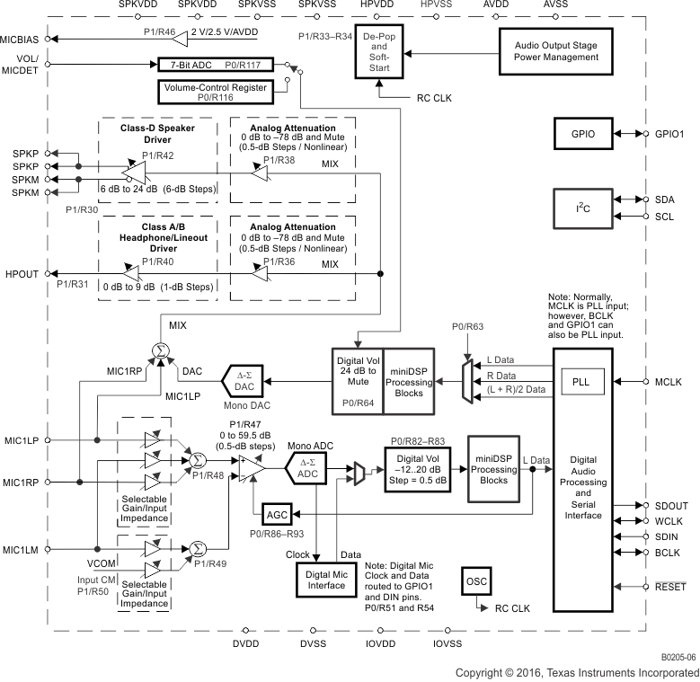
1.4 Functional Block Diagram
2 Revision History
Changes from B Revision (August 2016) to C Revision
- Added: Page 0 / Register 51 (0x33): GPIO1 In/Out Pin ControlGo
Changes from A Revision (May 2012) to B Revision
- Added ESD Ratings table, Feature Description section, Device Functional Modes, Application and Implementation section, Power Supply Recommendations section, Layout section, Device and Documentation Support section, and Mechanical, Packaging, and Orderable Information section.Go
- Deleted SPRVDD and SPRVSS pins from the Pin Functions tableGo
- Changed references to SPLVDD in Typical Performance graphs to SPKVDDGo
- Added Power-Supply Sequence section to the Device Initialization sectionGo
- Added the reference to the PGA Gain Versus Input Impedance table in the MICBIAS and Microphone Preamplifier sectionGo
- Changed SDIN terminal to DIN in Figure 7-16Go
- Changed Section 7.3.12.1.2 diagrams for PRB_P2/5/8/10/13/15/18/21/24/25 to reflect that the DRC_HPF filter cannot be bypassed when the DRC is turned off Go
- Added sequence for inserting a beep in the middle of an already-playing signal and note text following script in the Key-Click Functionality With Digital Sine-Wave Generator (PRB_P25) sectionGo
- Changed references of HPLOUT to HPOUT in Section 7.3.12.12.1 sectionGo
- Added PRB modes text to note for Page 0 / Register 20Go
- Added PRB modes text to Page 0 / Register 21. Also added Page 0 / Register 21 programmed value noteGo
- Added D(3:0) note to Page 0 / Register 22Go
- Changed last line to "10111-11000: Reserved. Do not use." "11001: DAC Signal Processing Block PRB_P25" "11010-11111: Reserved. Do not use."Go
- Changed values in Page 0 / Register 69 (0x45): DRC Control 2Go
- Changed Page 0, Register 70, bit D3-D0 decay rate value for 0000 from DR = 1.5625e–3 to DR = 0.015625Go
- Switched D1 and D0 descriptions so that D1 is for SP and D0 is for HP in Page 1 / Register 30 tableGo
- Changed Page 1 / Register 40, D1 to reservedGo
- Changed references to TLV320AIC3111 device to the TLV320AIC3120 device throughout the REGISTER MAP section Go
Changes from * Revision (February 2010) to A Revision
- Added PGA Gain table to data sheetGo
- Added PRB_P25 and values to Table 7-20.Go
- Added Section 7.3.12.1.2.9 and Signal Chain with beep generator imageGo
- Added section Section 7.3.12.7 after Interrupts sectionGo
- Added D6-D0 to the Register Value columns, and changed the Analog Attenuation columns to Analog GainGo
- Added table note to Analog Volume Control for Headphone and Speaker Outputs (for D7 = 1) tableGo
- Changed "page 0 / register 44" to " page 1 / register 44" in Headphone Drivers section Go
- Changed max AOSR values in Clock Distribution Tree image from 1023, 1024 to 255, 256.Go
- Changed PLL conditions under Equation 10 and Equation 11Go
- Added Timer sectionGo
- Deleted the Page 0 / Register 71–Page 0 / Register 80 table and added Beep Generator bit registers from SLAS659A (Page 0 / Register 71–80).Go
- Modified Page 0 / Register 80 title from Page 0 / Register 80-115: Reserved to Page 0 / Register 80: Reserved.Go
- Corrected values in Description column for bits D6–D0 of Page 0 / Register 83Go
- Changed Bit D0 = 1 to Reserved.Go
- Deleted references to Analog Volume Control (D7 = 0) table from Page 1 / Register 36 and Page 1 / Register 38Go
- Changed Added table note following Page 1 / Register 40Go
- Deleted one of the table notes from Page 1/ Register 48 and Page 1 / Register 49Go
3 Device Comparison
Table 3-1 Device Features Comparison
| FUNCTION | TLV320AIC3100 | TLV320AIC3110 | TLV320AIC3111 | TLV320AIC3120 |
|---|---|---|---|---|
| DACs | 2 | 2 | 2 | 1 |
| ADCs | 1 | 1 | 1 | 1 |
| Inputs / Outputs | 3/3 | 3/4 | 3/4 | 3/2 |
| Resolution (Bits) | 16, 20, 24, 32 | 16, 20, 24, 32 | 16, 20, 24, 32 | 16, 20, 24, 32 |
| Control Interface | I2C | I2C | I2C | I2C |
| Digital Audio Interface | LJ, RJ, I2S, TDM, DSP | LJ, RJ, I2S, TDM, DSP | LJ, RJ, I2S, TDM, DSP | LJ, RJ, I2S, TDM, DSP |
| Number of Digital Audio Interfaces | 1 | 1 | 1 | 1 |
| Speaker Amplifier Type | Mono Differential Class-D | Stereo Differential Class-D | Stereo Differential Class-D | Mono Differential Class-D |
| Configurable miniDSP | No | No | Yes | Yes |
| Headphone Driver | Yes | Yes | Yes | Yes |
4 Pin Configuration and Functions

4.1 Pin Attributes
Pin Functions
| PIN | I/O | DESCRIPTION | |
|---|---|---|---|
| NAME | NO. | ||
| AVDD | 17 | - | Analog power supply |
| AVSS | 16 | - | Analog ground |
| BCLK | 7 | I/O | Audio serial bit clock |
| DIN | 5 | I | Audio serial data input |
| DOUT | 4 | O | Audio serial data output |
| DVDD | 3 | - | Digital power – digital core |
| DVSS | 18 | - | Digital ground |
| GPIO1 | 32 | I/O | General-purpose input and output pin and multifunction pin |
| HPOUT | 27 | O | Mono headphone and line driver output |
| NC | 30 | O | No connection |
| HPVDD | 28 | - | Headphone/line driver and PLL power |
| HPVSS | 29 | - | Headphone/line driver and PLL ground |
| IOVDD | 2 | - | Interface power |
| IOVSS | 1 | - | Interface ground |
| MCLK | 8 | I | External master clock |
| MICBIAS | 12 | O | |
| MIC1LM | 15 | I | Microphone/line input routed to M or P input mixer |
| MIC1LP | 13 | I | Microphone/line input routed to P input mixer and left output mixer |
| MIC1RP | 14 | I | Microphone/line input routed to P input mixer and left/right output mixer |
| RESET | 31 | I | Device reset |
| SCL | 10 | I/O | I2C control bus clock input |
| SDA | 9 | I/O | I2C control-bus data input |
| SPKM | 19, 23 | I/O | Cass-D speaker driver inverting output |
| SPKP | 22, 26 | - | Class-D speaker driver noninverting output |
| SPKVDD | 21, 24 | - | Class-D speaker driver power supply |
| SPKVSS | 20, 25 | - | Class-D speaker driver power-supply ground |
| VOL/MICDET | 11 | I | Volume control or microphone detection |
| WCLK | 6 | I/O | Audio serial word clock |
5 Specifications
5.1 Absolute Maximum Ratings
over operating free-air temperature range (unless otherwise noted) (1)| MIN | MAX | UNIT | ||
|---|---|---|---|---|
| AVDD to AVSS | –0.3 | 3.9 | V | |
| DVDD to DVSS | –0.3 | 2.5 | V | |
| HPVDD to HPVSS | –0.3 | 3.9 | V | |
| SPKVDD to SPKVSS | –0.3 | 6 | V | |
| IOVDD to IOVSS | –0.3 | 3.9 | V | |
| Digital input voltage | IOVSS – 0.3 | IOVDD + 0.3 | V | |
| Analog input voltage | AVSS – 0.3 | AVDD + 0.3 | V | |
| Operating temperature | –40 | 85 | °C | |
| Junction temperature (TJ Max) | 105 | °C | ||
| Storage temperature, Tstg | –55 | 150 | °C | |
| Power dissipation | (TJ Max – TA) / RθJA | °C | ||
| RθJA Thermal impedance (with thermal pad soldered to board) | 35 | °C/W | ||
5.2 ESD Ratings
| VALUE | UNIT | |||
|---|---|---|---|---|
| V(ESD) | Electrostatic discharge | Human-body model (HBM), per ANSI/ESDA/JEDEC JS-001(1) | ±2000 | V |
| Charged-device model (CDM), per JEDEC specification JESD22-C101(2) | ±1000 | |||
5.3 Recommended Operating Conditions
over operating free-air temperature range (unless otherwise noted)| MIN | NOM | MAX | UNIT | |||
|---|---|---|---|---|---|---|
| AVDD(2) | Power-supply voltage | Referenced to AVSS(1) | 2.7 | 3.3 | 3.6 | V |
| DVDD | Referenced to DVSS(1) | 1.65 | 1.8 | 1.95 | ||
| HPVDD | Referenced to HPVSS(1) | 2.7 | 3.3 | 3.6 | ||
| SPKVDD(2) | Referenced to SPKVSS(1) | 2.7 | 5.5 | |||
| IOVDD | Referenced to IOVSS(1) | 1.1 | 3.3 | 3.6 | ||
| Speaker impedance | Resistance applied across class-D ouput pins (BTL) | 4 | Ω | |||
| Headphone impedance | AC coupled to RL | 16 | Ω | |||
| VI | Analog audio full-scale input voltage | AVDD = 3.3 V, single-ended | 0.707 | VRMS | ||
| Mono line output load impedance | AC coupled to RL | 10 | kΩ | |||
| MCLK(3) | Master clock frequency | IOVDD = 3.3 V | 50 | MHz | ||
| SCL | SCL clock frequency | 400 | kHz | |||
| TA | Operating free-air temperature | –40 | 85 | °C | ||
5.4 Thermal Information
| THERMAL METRIC(1) | TLV320AIC3120 | UNIT | ||
|---|---|---|---|---|
| RHB (VQFN) | ||||
| 32 PINS | ||||
| RθJA | Junction-to-ambient thermal resistance | 32.7 | °C/W | |
| RθJC(top) | Junction-to-case (top) thermal resistance | 23.2 | °C/W | |
| RθJB | Junction-to-board thermal resistance | 6.6 | °C/W | |
| ψJT | Junction-to-top characterization parameter | 0.3 | °C/W | |
| ψJB | Junction-to-board characterization parameter | 6.5 | °C/W | |
| RθJC(bot) | Junction-to-case (bottom) thermal resistance | 2 | °C/W | |
5.5 Electrical Characteristics
At 25°C, AVDD = HPVDD = IOVDD = 3.3 V, SPKVDD = 3.6V, DVDD = 1.8 V, fS (audio) = 48 kHz, CODEC_CLKIN = 256 × fS, PLL = Off, VOL/MICDET pin disabled (unless otherwise noted)| PARAMETER | TEST CONDITIONS | MIN | TYP | MAX | UNIT | |
|---|---|---|---|---|---|---|
| INTERNAL OSCILLATOR-RC_CLK | ||||||
| Oscillator frequency | 8.2 | MHz | ||||
| VOLUME CONTROL PIN (ADC); VOL/MICDET pin enabled | ||||||
| Input voltage range | VOL/MICDET pin configured as volume control (page 0 / register 116, bit D7 = 1 and page 0 / register 67, bit D7 = 0) | 0 | 0.5 x AVDD | V | ||
| Input capacitance | 2 | pF | ||||
| Volume control steps | 128 | Steps | ||||
| AUDIO ADC | ||||||
| Microphone Input to ADC, 984-Hz Sine-Wave Input, fS = 48 kHz, AGC = OFF | ||||||
| Input signal level (0-dB) | MIC with R1 = 20 kΩ (page 1 / register 48 and register 49, bits D7-D6) | 0.707 | VRMS | |||
| SNR | Signal-to-noise ratio | fS = 48 kHz, 0-dB PGA gain, MIC input ac-shorted to ground; measured as idle-channel noise, A-weighted(1) (2) | 80 | 91 | dB | |
| Dynamic range | fS = 48 kHz, 0-dB PGA gain, MIC input 1 kHz at –60-dBFS input applied, referenced to 0.707-VRMS input, A-weighted(1) (2) | 91 | dB | |||
| THD+N | Total harmonic distortion + noise | fS = 48 kHz, 0-dB PGA gain, MIC input 1 kHz at –2 dBFS input applied, referenced to 0.707-VRMS input | –85 | –70 | dB | |
| THD | Total harmonic distortion | fS = 48 kHz, 0-dB PGA gain, MIC input 1 kHz at –2 dBFS input applied, referenced to 0.707-VRMS input | –91 | dB | ||
| Input capacitance | MIC input | 2 | pF | |||
| Microphone Bias | ||||||
| Voltage output | Page 1 / register 46, bits D1–D0 = 10 | 2.25 | 2.5 | 2.75 | V | |
| Page 1 / register 46, bits D1–D0 = 01 | 2 | |||||
| Voltage regulation | At 4-mA load current, page 1 / register 46, bits D1–D0 = 10 (MICBIAS = 2.5 V) | 5 | mV | |||
| At 4-mA load current, page 1 / register 46, bits D1–D0 = 01 (MICBIAS = 2 V) | 7 | |||||
| Audio ADC Digital Decimation Filter Characteristics | ||||||
| See Section 7.3.10.4.4 for audio ADC decimation filter characteristics. | ||||||
| DAC HEADPHONE OUTPUT, AC-coupled load = 16 Ω (single-ended), driver gain = 0 dB, parasitic capacitance = 30 pF | ||||||
| Full-scale output voltage (0 dB) | Output common-mode setting = 1.65 V | 0.707 | VRMS | |||
| SNR | Signal-to-noise ratio | Measured as idle-channel noise, A-weighted(1) (2) | 80 | 95 | dB | |
| THD | Total harmonic distortion | 0-dBFS input | –85 | –65 | dB | |
| THD+N | Total harmonic distortion + noise | 0-dBFS input | –82 | –60 | dB | |
| Mute attenuation | 87 | dB | ||||
| PSRR | Power-supply rejection ratio(4) | Ripple on HPVDD (3.3 V) = 200 mVp-p at 1 kHz | –62 | dB | ||
| PO | Maximum output power | RL = 32 Ω, THD+N = –60 dB | 20 | mW | ||
| RL = 16 Ω, THD+N = –60 dB | 60 | |||||
| DAC LINEOUT (HP Driver in Lineout Mode) | ||||||
| SNR | Signal-to-noise ratio | Measured as idle-channel noise, A-weighted | 95 | dB | ||
| THD | Total harmonic distortion | 0-dBFS input, 0-dB gain | –86 | dB | ||
| THD+N | Total harmonic distortion + noise | 0-dBFS input, 0-dB gain | –83 | dB | ||
| DAC Digital Interpolation Filter Characteristics | ||||||
| See Section 7.3.12.1.4 for DAC interpolation filter characteristics. | ||||||
| DAC Output to Class-D SPEAKER OUTPUT; Load = 4 Ω (Differential), 50 pF | ||||||
| Output voltage | SPKVDD = 3.6 V, BTL measurement, DAC input = 0 dBFS, CM = 1.8 V, class-D gain = 6 dB, THD = –16.5 dB | 2.3 | VRMS | |||
| SPKVDD = 3.6 V, BTL measurement, DAC input = –2 dBFS, CM = 1.8 V, class-D gain = 6 dB, THD = –20 dB | 2.1 | |||||
| Output, common-mode | SPKVDD = 3.6 V, BTL measurement, DAC input = mute, class-D gain = 6 dB | 1.8 | V | |||
| SNR | Signal-to-noise ratio | SPKVDD = 3.6 V, BTL measurement, class-D gain = 6 dB, measured as idle-channel noise, A-weighted (with respect to full-scale output value of 2.3 VRMS)(1) (2) | 88 | dB | ||
| THD | Total harmonic distortion | –65 | dB | |||
| THD+N | Total harmonic distortion + noise | SPKVDD = 3.6 V, BTL measurement, DAC input = –6 dBFS, CM = 1.8 V, class-D gain = 6 dB | –63 | dB | ||
| PSRR | Power-supply rejection ratio(3) | SPKVDD = 3.6 V, BTL measurement, ripple on SPKVDD = 200 mVp-p at 1 kHz | –44 | dB | ||
| Mute attenuation | 110 | dB | ||||
| PO | Maximum output power | SPKVDD = 3.6 V, BTL measurement, CM = 1.8 V, class-D gain = 18 dB, THD = 10% | 1 | W | ||
| SPKVDD = 4.3 V, BTL measurement, CM = 1.8 V, class-D gain = 18 dB, THD = 10% | 1.5 | W | ||||
| SPKVDD = 5.5 V, BTL measurement, CM = 1.8 V, class-D gain = 18 dB, THD = 10% | 2.5 | W | ||||
| DAC OUTPUT to CLASS-D SPEAKER OUTPUT; Load = 8 Ω (Differential), 50 pF | ||||||
| Output voltage | SPKVDD = 3.6 V, BTL measurement, DAC input = 0 dBFS, CM = 1.8 V, class-D gain = 6 dB, THD = –16.5 dB | 2.2 | VRMS | |||
| SPKVDD = 3.6 V, BTL measurement, DAC input = –2 dBFS, CM = 1.8 V, class-D gain = 6 dB, THD = –20 dB | 2.1 | VRMS | ||||
| Output, common-mode | SPKVDD = 3.6 V, BTL measurement, DAC input = mute, class-D gain = 6 dB | 1.8 | V | |||
| SNR | Signal-to-noise ratio | SPKVDD = 3.6 V, BTL measurement, class-D gain = 6 dB, measured as idle-channel noise, A-weighted (with respect to full-scale output value of 2.2 VRMS) | 87 | dB | ||
| THD | Total harmonic distortion | SPKVDD = 3.6 V, BTL measurement, DAC input = –6 dBFS, CM = 1.8 V, class-D gain = 6 dB | –67 | dB | ||
| THD+N | Total harmonic distortion + noise | SPKVDD = 3.6 V, BTL measurement, DAC input = –6 dBFS, CM = 1.8 V, class-D gain = 6 dB | –66 | dB | ||
| PSRR | Power-supply rejection ratio(3) | SPKVDD = 3.6 V, BTL measurement, ripple on SPKVDD = 200 mVp-p at 1 kHz | –44 | dB | ||
| Mute attenuation | 110 | dB | ||||
| PO | Maximum output power | SPKVDD = 3.6 V, BTL measurement, CM = 1.8 V, class-D gain = 18 dB, THD = 10% | 0.7 | W | ||
| SPKVDD = 4.3 V, BTL measurement, CM = 1.8 V, class-D gain = 18 dB, THD = 10% | 1 | |||||
| SPKVDD = 5.5 V, BTL measurement, CM = 1.8 V, class-D gain = 18 dB, THD = 10% | 1.6 | |||||
| Output-stage leakage current for direct battery connection | SPKVDD = 4.3 V, device is powered down (power-up-reset condition) | 80 | nA | |||
| ADC and DAC POWER CONSUMPTION | ||||||
| For ADC and DAC power consumption based per selected processing block, see Section 7.3.9. | ||||||
| DIGITAL INPUT/OUTPUT | ||||||
| Logic family | CMOS | |||||
| VIH | Logic Level | IIH = 5 µA, IOVDD = 1.6 V | 0.7 × IOVDD | V | ||
| IIH = 5 µA, IOVDD = 1.6 V | IOVDD | |||||
| VIL | IIL = 5 µA, IOVDD = 1.6 V | –0.3 | 0.3 × IOVDD | |||
| IIL = 5 µA, IOVDD = 1.6 V | 0 | |||||
| VOH | IOH = 2 TTL loads | 0.8 × IOVDD | ||||
| VOL | IOL = 2 TTL loads | 0.1 × IOVDD | ||||
| Capacitive load | 10 | pF | ||||
5.6 Power Dissipation Ratings(1)
This data was taken using 2-oz. (0,071-mm thick) trace and copper pad that is soldered to a JEDEC high-K, standard 4-layer 3-inch × 3-inch (7,62-cm × 7,62-cm) PCB.| Power Rating at 25°C | Derating Factor | Power Rating at 70°C | Power Rating at 85°C |
|---|---|---|---|
| 2.3 W | 28.57 mW/°C | 1 W | 0.6 W |
5.7 I2S, LJF, and RJF Timing in Master Mode
All specifications at 25°C, DVDD = 1.8 V. Note: All timing specifications are measured at characterization but not tested at final test. See Figure 5-1.| PARAMETER | IOVDD = 1.1 V | IOVDD = 3.3 V | UNIT | |||
|---|---|---|---|---|---|---|
| MIN | MAX | MIN | MAX | |||
| td(WS) | WCLK delay | 45 | 20 | ns | ||
| td(DO-WS) | WCLK to DOUT delay (for LJF mode only) | 45 | 20 | ns | ||
| td(DO-BCLK) | BCLK to DOUT delay | 45 | 20 | ns | ||
| ts(DI) | DIN setup | 8 | 6 | ns | ||
| th(DI) | DIN hold | 8 | 6 | ns | ||
| tr | Rise time | 25 | 10 | ns | ||
| tf | Fall time | 25 | 10 | ns | ||
5.8 I2S, LJF, and RJF Timing in Slave Mode
All specifications at 25°C, DVDD = 1.8 V. Note: All timing specifications are measured at characterization but not tested at final test. See Figure 5-2.| PARAMETER | IOVDD = 1.1 V | IOVDD = 3.3 V | UNIT | |||
|---|---|---|---|---|---|---|
| MIN | MAX | MIN | MAX | |||
| tH(BCLK) | BCLK high period | 35 | 35 | ns | ||
| tL(BCLK) | BCLK low period | 35 | 35 | ns | ||
| ts(WS) | WCLK setup | 8 | 6 | ns | ||
| th(WS) | WCLK hold | 8 | 6 | ns | ||
| td(DO-WS) | WCLK to DOUT delay (for LJF mode only) | 45 | 20 | ns | ||
| td(DO-BCLK) | BCLK to DOUT delay | 45 | 20 | ns | ||
| ts(DI) | DIN setup | 8 | 6 | ns | ||
| th(DI) | DIN hold | 8 | 6 | ns | ||
| tr | Rise time | 4 | 4 | ns | ||
| tf | Fall time | 4 | 4 | ns | ||
5.9 DSP Timing in Master Mode
All specifications at 25°C, DVDD = 1.8 V. Note: All timing specifications are measured at characterization but not tested at final test. See Figure 5-3.| PARAMETER | IOVDD = 1.1 V | IOVDD = 3.3 V | UNIT | |||
|---|---|---|---|---|---|---|
| MIN | MAX | MIN | MAX | |||
| td(WS) | WCLK delay | 45 | 20 | ns | ||
| td(DO-BCLK) | BCLK to DOUT delay | 45 | 20 | ns | ||
| ts(DI) | DIN setup | 8 | 8 | ns | ||
| th(DI) | DIN hold | 8 | 8 | ns | ||
| tr | Rise time | 25 | 10 | ns | ||
| tf | Fall time | 25 | 10 | ns | ||
5.10 DSP Timing in Slave Mode
All specifications at 25°C, DVDD = 1.8 V. Note: All timing specifications are measured at characterization but not tested at final test. See Figure 5-4.| PARAMETER | IOVDD = 1.1 V | IOVDD = 3.3 V | UNIT | |||
|---|---|---|---|---|---|---|
| MIN | MAX | MIN | MAX | |||
| tH(BCLK) | BCLK high period | 35 | 35 | ns | ||
| tL(BCLK) | BCLK low period | 35 | 35 | ns | ||
| ts(WS) | WCLK setup | 8 | 8 | ns | ||
| th(WS) | WCLK hold | 8 | 8 | ns | ||
| td(DO-BCLK) | BCLK to DOUT delay | 45 | 20 | ns | ||
| ts(DI) | DIN setup | 8 | 8 | ns | ||
| th(DI) | DIN hold | 8 | 8 | ns | ||
| tr | Rise time | 4 | 4 | ns | ||
| tf | Fall time | 4 | 4 | ns | ||
5.11 I2C Interface Timing
All specifications at 25°C, DVDD = 1.8 V. Note: All timing specifications are measured at characterization.See Figure 5-5.| PARAMETER | Standard Mode | Fast Mode | UNIT | |||||
|---|---|---|---|---|---|---|---|---|
| MIN | TYP | MAX | MIN | TYP | MAX | |||
| fSCL | SCL clock frequency | 0 | 100 | 0 | 400 | kHz | ||
| tHD;STA | Hold time (repeated) START condition. After this period, the first clock pulse is generated. | 4 | 0.8 | μs | ||||
| tLOW | LOW period of the SCL clock | 4.7 | 1.3 | μs | ||||
| tHIGH | HIGH period of the SCL clock | 4 | 0.6 | μs | ||||
| tSU;STA | Setup time for a repeated START condition | 4.7 | 0.8 | μs | ||||
| tHD;DAT | Data hold time: for I2C bus devices | 0 | 3.45 | 0 | 0.9 | μs | ||
| tSU;DAT | Data set-up time | 250 | 100 | ns | ||||
| tr | SDA and SCL rise time | 1000 | 20 + 0.1Cb | 300 | ns | |||
| tf | SDA and SCL fall time | 300 | 20 + 0.1Cb | 300 | ns | |||
| tSU;STO | Set-up time for STOP condition | 4 | 0.8 | μs | ||||
| tBUF | Bus free time between a STOP and START condition | 4.7 | 1.3 | μs | ||||
| Cb | Capacitive load for each bus line | 400 | 400 | pF | ||||
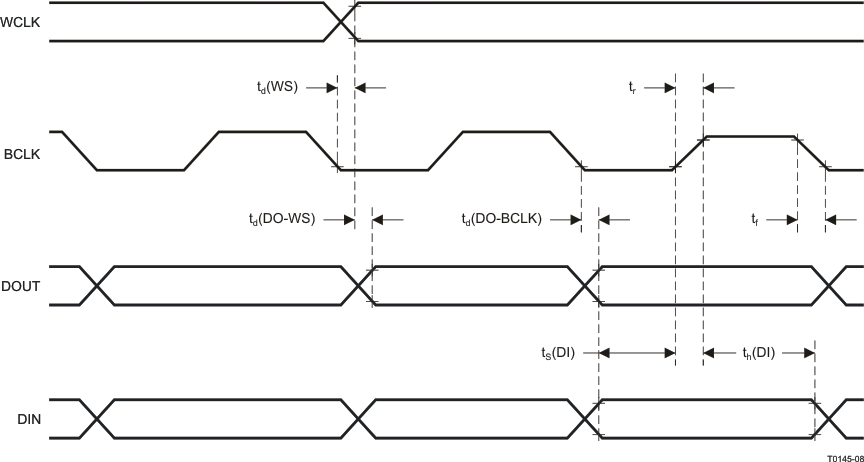 Figure 5-1 I2S/LJF/RJF Timing in Master Mode
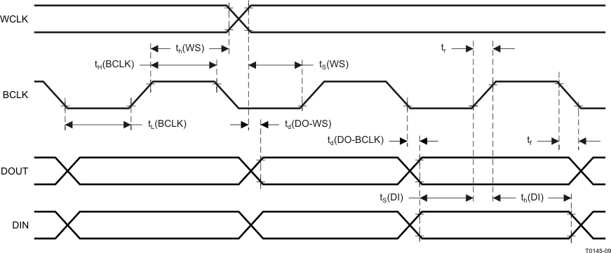 Figure 5-2 I2S/LJF/RJF Timing in Slave Mode
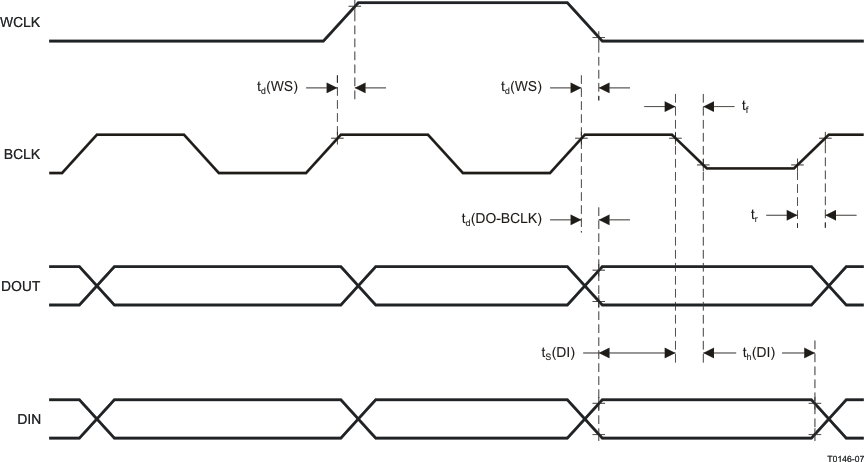 Figure 5-3 DSP Timing in Master Mode
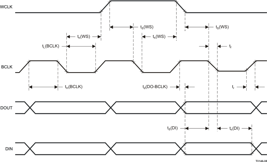 Figure 5-4 DSP Timing in Slave Mode
 Figure 5-5 I2C Interface Timing Diagram
5.12 Typical Characteristics
5.12.1 Audio ADC Performance
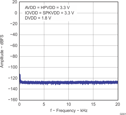
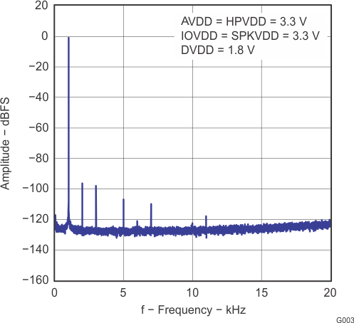 Figure 5-8 Amplitude vs Frequency
FFT – ADC Differential Input
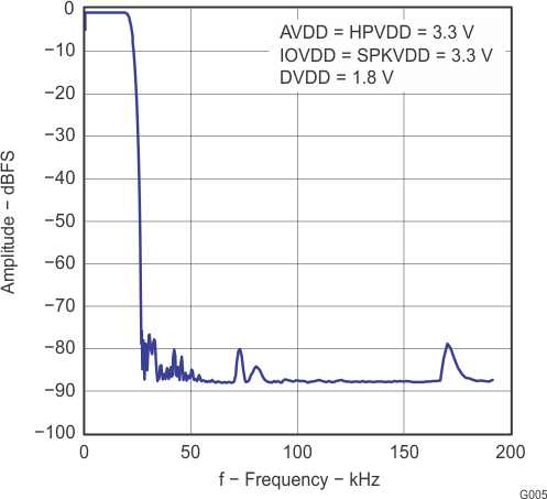 Figure 5-10 Amplitude vs Frequency
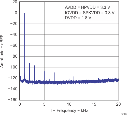 Figure 5-7 Amplitude vs Frequency
FFT – ADC Single-Ended Input
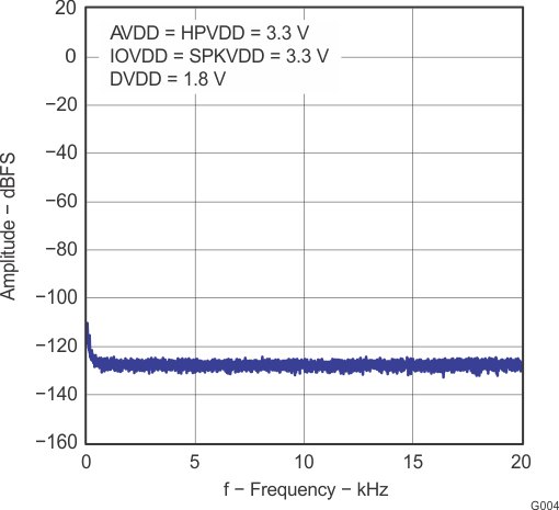 Figure 5-9 Amplitude vs Frequency
FFT – ADC Idle Channel, Single-Ended
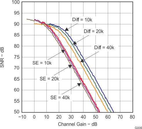 Figure 5-11 SNR vs PGA Channel Gain
5.12.2 DAC Performance
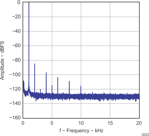 Figure 5-12 Amplitude vs Frequency
FFT - DAC to Line Output
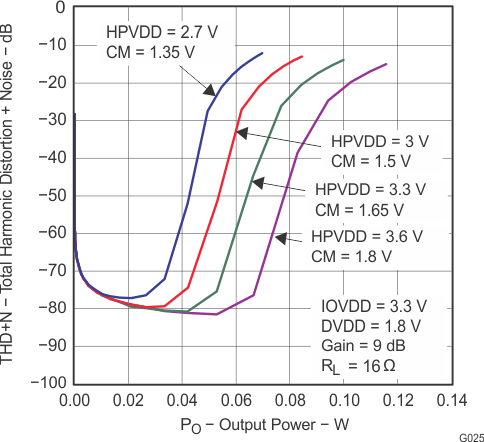 Figure 5-14 Total Harmonic Distortion + Noise vs Output Power
Headphone Output Power
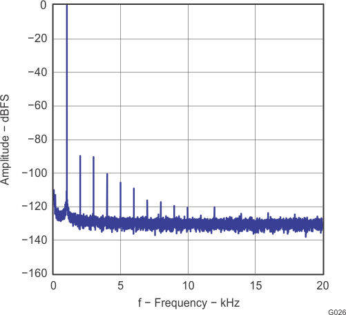 Figure 5-13 Amplitude vs Frequency
FFT - DAC to Headphone Output
5.12.3 Class-D Speaker Driver Performance
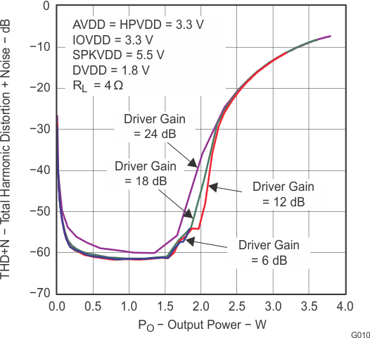 Figure 5-15 Total Harmonic Distortion + Noise vs Output Power
Max Class-D Speaker-Driver Output Power (RL = 4 Ω)
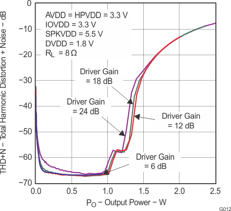 Figure 5-17 Total Harmonic Distortion + Noise vs Output Power
Max Class-D Speaker-Driver Output Power (RL = 8 Ω)
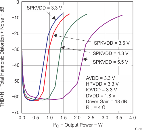 Figure 5-16 Total Harmonic Distortion + Noise vs Output Power
Class-D Speaker-Driver Output Power (RL = 4 Ω)
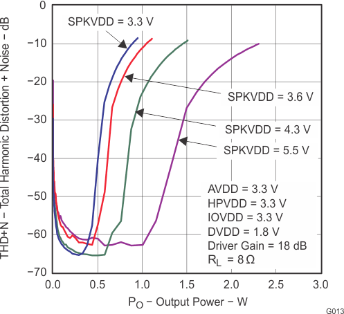 Figure 5-18 Total Harmonic Distortion + Noise vs Output Power
Class-D Speaker-Driver Output Power (RL = 8 Ω)
5.12.4 Analog Bypass Performance
H
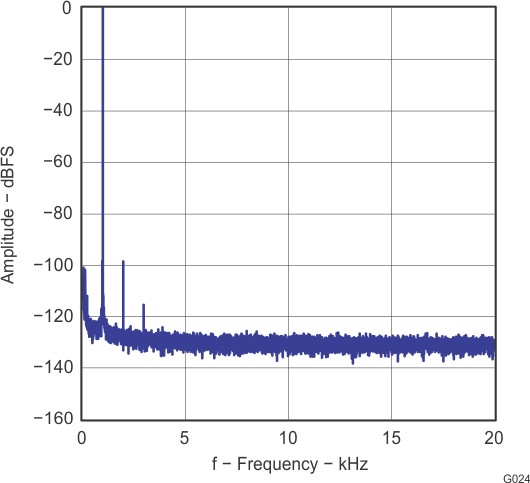 Figure 5-19 Amplitude vs Frequency
FFT - Line-In Bypass to Line Output
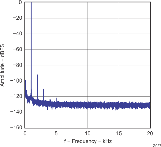 Figure 5-20 Amplitude vs Frequency
FFT - Line-In Bypass to Headphone Output
5.12.5 MICBIAS Performance
H
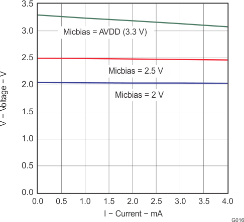 Figure 5-21 Voltage vs Current
MICBIAS
