SLLSEQ2A September 2016 – December 2016
PRODUCTION DATA.
- 1 Features
- 2 Applications
- 3 Description
- 4 Revision History
- 5 Description (continued)
- 6 Pin Configuration and Function
-
7 Specifications
- 7.1 Absolute Maximum Ratings
- 7.2 ESD Ratings
- 7.3 Recommended Operating Conditions
- 7.4 Thermal Information
- 7.5 Power Ratings
- 7.6 Insulation Specifications
- 7.7 Safety-Related Certifications
- 7.8 Safety Limiting Values
- 7.9 Electrical Characteristics
- 7.10 Switching Characteristics
- 7.11 Insulation Characteristics Curves
- 7.12 Typical Characteristics
- 8 Parameter Measurement Information
- 9 Detailed Description
-
10Application and Implementation
- 10.1 Application Information
- 10.2
Typical Applications
- 10.2.1 Design Requirements
- 10.2.2
Detailed Design Procedure
- 10.2.2.1 Recommended ISO5852S-Q1 Application Circuit
- 10.2.2.2 FLT and RDY Pin Circuitry
- 10.2.2.3 Driving the Control Inputs
- 10.2.2.4 Local Shutdown and Reset
- 10.2.2.5 Global-Shutdown and Reset
- 10.2.2.6 Auto-Reset
- 10.2.2.7 DESAT Pin Protection
- 10.2.2.8 DESAT Diode and DESAT Threshold
- 10.2.2.9 Determining the Maximum Available, Dynamic Output Power, POD-max
- 10.2.2.10 Example
- 10.2.2.11 Higher Output Current Using an External Current Buffer
- 10.2.3 Application Curves
- 11Power Supply Recommendations
- 12Layout
- 13Device and Documentation Support
- 14Mechanical, Packaging, and Orderable Information
1 Features
- Qualified for Automotive Applications
- AEC-Q100 Qualified With the Following Results:
- Device Temperature Grade 1: –40°C to +125°C Ambient Operating Temperature Range
- Device HBM Classification Level 3A
- Device CDM Classification Level C6
- 100-kV/μs Minimum Common-Mode Transient Immunity (CMTI) at VCM = 1500 V
- Split Outputs to Provide 2.5-A Peak Source and
5-A Peak Sink Currents - Short Propagation Delay: 76 ns (Typ),
110 ns (Max) - 2-A Active Miller Clamp
- Output Short-Circuit Clamp
- Soft Turn-Off (STO) during Short Circuit
- Fault Alarm upon Desaturation Detection is Signaled on FLT and Reset Through RST
- Input and Output Undervoltage Lockout (UVLO) with Ready (RDY) Pin Indication
- Active Output Pulldown and Default Low Outputs with Low Supply or Floating Inputs
- 2.25-V to 5.5-V Input Supply Voltage
- 15-V to 30-V Output Driver Supply Voltage
- CMOS Compatible Inputs
- Rejects Input Pulses and Noise Transients Shorter Than 20 ns
- Isolation Surge Withstand Voltage 12800-VPK
- Safety-Related Certifications:
- 8000-VPK VIOTM and 2121-VPK VIORM Reinforced Isolation per DIN V VDE V 0884-10 (VDE V 0884-10):2006-12
- 5700-VRMS Isolation for 1 Minute per UL 1577
- CSA Component Acceptance Notice 5A, IEC 60950–1 and IEC 60601–1 End Equipment Standards
- TUV Certification per EN 61010-1 and EN 60950-1
- GB4943.1-2011 CQC Certification
- All Certifications Complete per UL, VDE, CQC, TUV and Planned for CSA
2 Applications
- Isolated IGBT and MOSFET Drives in:
- HEV and EV Power Modules
- Industrial Motor Control Drives
- Industrial Power Supplies
- Solar Inverters
- Induction Heating
3 Description
The ISO5852S-Q1 device is a 5.7-kVRMS, reinforced isolated gate driver for IGBTs and MOSFETs with split outputs, OUTH and OUTL, providing 2.5-A source and 5-A sink current. The input side operates from a single 2.25-V to 5.5-V supply. The output side allows for a supply range from minimum 15 V to maximum 30 V. Two complementary CMOS inputs control the output state of the gate driver. The short propagation time of 76 ns provides accurate control of the output stage.
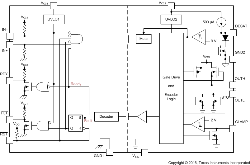
An internal desaturation (DESAT) fault detection recognizes when the IGBT is in an overcurrent condition. Upon a DESAT detect, a mute logic immediately blocks the output of the isolator and initiates a soft-turnoff procedure which disables the OUTH pin and pulls the OUTL pin to low over a time span of 2 μs. When the OUTL pin reaches 2 V with respect to the most-negative supply potential, VEE2, the gate-driver output is pulled hard to the VEE2 potential, turning the IGBT immediately off.
Device Information(1)
| PART NUMBER | PACKAGE | BODY SIZE (NOM) |
|---|---|---|
| ISO5852S-Q1 | SOIC (16) | 10.30 mm × 7.50 mm |
- For all available packages, see the orderable addendum at the end of the data sheet.
Functional Block Diagram
