-
ISO7821LLS High-Performance, 8000-VPK Reinforced Isolated Dual-LVDS Buffer
- 1 Features
- 2 Applications
- 3 Description
- 4 Revision History
- 5 Pin Configuration and Functions
-
6 Specifications
- 6.1 Absolute Maximum Ratings
- 6.2 ESD Ratings
- 6.3 Recommended Operating Conditions
- 6.4 Thermal Information
- 6.5 Power Ratings
- 6.6 Insulation Specifications
- 6.7 Safety-Related Certifications
- 6.8 Safety Limiting Values
- 6.9 DC Electrical Characteristics
- 6.10 DC Supply Current Characteristics
- 6.11 Timing Requirements for Distortion Correction Scheme
- 6.12 Switching Characteristics
- 6.13 Insulation Characteristics Curves
- 6.14 Typical Characteristics
- 7 Parameter Measurement Information
- 8 Detailed Description
- 9 Application and Implementation
- 10Power Supply Recommendations
- 11Layout
- 12Device and Documentation Support
- 13Mechanical, Packaging, and Orderable Information
- IMPORTANT NOTICE
ISO7821LLS High-Performance, 8000-VPK Reinforced Isolated Dual-LVDS Buffer
1 Features
- Complies with TIA/EIA-644-A LVDS Standard
- Signaling Rate: 50 Mbps to 150 Mbps
- Optimized for DC-Balanced Data
- Wide Supply Range: 3 V to 5.5 V
- Wide Temperature Range: –55°C to 125°C
- Low-Power Consumption, Typical 10.3 mA per Channel at 150 Mbps
- Low Propagation Delay: 17 ns Typical
- Industry leading CMTI(Min): ±100 kV/μs
- Robust Electromagnetic Compatibility (EMC)
- System-Level ESD, EFT, and Surge Immunity
- Low Emissions
- Isolation Barrier Life: > 40 Years
- SOIC-16 Wide Body (DW) and Extra-Wide Body (DWW) Package Options
- Isolation Surge Withstand Voltage 12800 VPK
- Safety-Related Certifications:
- 8000-VPK Reinforced Isolation per DIN V VDE V 0884–10 (VDE V 0884–10): 2006–12
- 5700-VRMS Isolation for 1 minute per UL 1577
- CSA Component Acceptance Notice 5A, IEC 60950–1 and IEC 60601–1 End Equipment Standards
- TUV Certification per EN 61010-1 and EN 60950-1
- CQC Certification per GB4943.1–2011
- All Certifications are Planned
2 Applications
- Motor Control
- Test and Measurement
- Industrial Automation
- Medical Equipment
- Communication Systems
3 Description
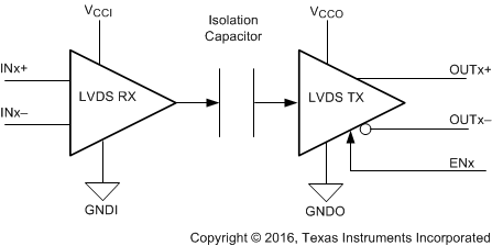
The ISO7821LLS device is a high-performance, isolated dual-LVDS buffer with 8000-VPK isolation voltage. This device provides high electromagnetic immunity and low emissions at low-power consumption, while isolating the LVDS bus signal. Each isolation channel has an LVDS receive and transmit buffer. Timing performance for the ISO7821LLS device is optimized for use with communication systems that use DC-balanced data streams which is achieved through an internal distortion correction scheme.
The ISO7821LLS device has one forward and one reverse-direction channel.
Through innovative chip design and layout techniques, the electromagnetic compatibility of the ISO7821LLS device has been significantly enhanced to ease system-level ESD, EFT, surge, and emissions compliance.
The ISO7821LLS device is available in a 16-pin SOIC wide-body (DW) and extra-wide body (DWW) packages.
Device Information(1)
| PART NUMBER | PACKAGE | BODY SIZE (NOM) |
|---|---|---|
| ISO7821LLS | DW (16) | 10.30 mm × 7.50 mm |
| DWW (16) | 10.30 mm × 14.00 mm |
- For all available packages, see the orderable addendum at the end of the data sheet.
Simplified Schematic
4 Revision History
Changes from * Revision (March 2016) to A Revision
- Changed the device status from Product Preview to Production Data and released full version of the data sheetGo
5 Pin Configuration and Functions
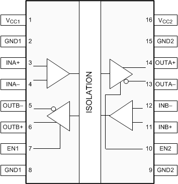
Pin Functions
| PIN | I/O | DESCRIPTION | |
|---|---|---|---|
| NAME | NO. | ||
| EN1 | 7 | I | Output enable 1. Output pins on side 1 are enabled when EN1 is high or open and in high impedance state when EN1 is low. |
| EN2 | 10 | I | Output enable 2. Output pins on side 2 are enabled when EN2 is high or open and in high impedance state when EN2 is low. |
| GND1 | 2 | — | Ground connection for VCC1 |
| 8 | |||
| GND2 | 9 | — | Ground connection for VCC2 |
| 15 | |||
| INA+ | 3 | I | Positive differential input, channel A |
| INA– | 4 | I | Negative differential input, channel A |
| INB+ | 11 | I | Positive differential input, channel B |
| INB– | 12 | I | Negative differential input, channel B |
| OUTA+ | 14 | O | Positive differential output, channel A |
| OUTA– | 13 | O | Negative differential output, channel A |
| OUTB+ | 6 | O | Positive differential output, channel B |
| OUTB– | 5 | O | Negative differential output, channel B |
| VCC1 | 1 | — | Power supply, side 1, VCC1 |
| VCC2 | 16 | — | Power supply, side 2, VCC2 |
6 Specifications
6.1 Absolute Maximum Ratings
over operating free-air temperature range (unless otherwise noted)(1)| MIN | MAX | UNIT | |||
|---|---|---|---|---|---|
| VCCx | Supply voltage(2) | VCC1, VCC2 | –0.5 | 6 | V |
| V | Voltage on input, output, and enable pins | OUTx, INx, ENx | –0.5 | VCCx + 0.5(3) | V |
| IO | Maximum current through OUTx pins | –20 | 20 | mA | |
| TJ | Junction temperature | –55 | 150 | °C | |
| Tstg | Storage temperature | –65 | 150 | °C | |
6.2 ESD Ratings
| VALUE | UNIT | |||
|---|---|---|---|---|
| V(ESD) | Electrostatic discharge | Human-body model (HBM), per ANSI/ESDA/JEDEC JS-001(1) | ±4500 | V |
| Charged-device model (CDM), per JEDEC specification JESD22-C101(2) | ±1500 | |||
6.3 Recommended Operating Conditions
| MIN | NOM | MAX | UNIT | |||
|---|---|---|---|---|---|---|
| VCC1, VCC2 | Supply voltage | 3 | 3.3 | 5.5 | V | |
| |VID| | Magnitude of RX input differential voltage | Driven with voltage sources on RX pins | 100 | 600 | mV | |
| VIC | RX input common-mode voltage | VCC1, VCC2 ≥ 3 V | 0.5 |VID| | 2.4 – 0.5 |VID| | V | |
| RL | TX far-end differential termination | 100 | Ω | |||
| DR | Signaling rate | 50 | 150 | Mbps | ||
| TA | Ambient temperature | –55 | 25 | 125 | °C | |
6.4 Thermal Information
| THERMAL METRIC(1) | ISO7821LLS | UNIT | |||
|---|---|---|---|---|---|
| DW (SOIC) | DWW (SOIC) | ||||
| 16 PINS | 16 PINS | ||||
| RθJA | Junction-to-ambient thermal resistance | 82 | 84.6 | °C/W | |
| RθJC(top) | Junction-to-case(top) thermal resistance | 44.6 | 46.4 | °C/W | |
| RθJB | Junction-to-board thermal resistance | 46.6 | 55.3 | °C/W | |
| ψJT | Junction-to-top characterization parameter | 17.8 | 18.7 | °C/W | |
| ψJB | Junction-to-board characterization parameter | 46.1 | 54.5 | °C/W | |
| RθJC(bottom) | Junction-to-case(bottom) thermal resistance | — | — | °C/W | |
6.5 Power Ratings
VCC1 = VCC2 = 5.5 V, TJ = 150°C, CL = 5 pF, RL = 100-Ω differential, input a 75-MHz 50% duty-cycle square wave,EN1 = EN2 = 5.5 V
| PARAMETER | TEST CONDITIONS | MAX | TYP | MAX | UNIT | |
|---|---|---|---|---|---|---|
| PD | Maximum power dissipation (both sides) | 180 | mW | |||
| PD1 | Maximum power dissipation (side 1) | 90 | mW | |||
| PD2 | Maximum power dissipation (side 2) | 90 | mW | |||
6.6 Insulation Specifications
over operating free-air temperature range (unless otherwise noted)| PARAMETER | TEST CONDITIONS | SPECIFICATION | UNIT | ||
|---|---|---|---|---|---|
| DW | DWW | ||||
| GENERAL | |||||
| CLR | External clearance(1) | Shortest terminal-to-terminal distance through air | >8 | >14.5 | mm |
| CPG | External creepage(1) | Shortest terminal-to-terminal distance across the package surface | >8 | >14.5 | mm |
| DTI | Distance through the insulation | Minimum internal gap (internal clearance) | >21 | >21 | μm |
| CTI | Tracking resistance (comparative tracking index) | DIN EN 60112 (VDE 0303–11); IEC 60112; UL 746A | >600 | >600 | V |
| Material group | According to IEC 60664-1 | I | I | ||
| Overvoltage category per IEC 60664-1 | Rated mains voltage ≤ 600 VRMS | I–IV | I–IV | ||
| Rated mains voltage ≤ 1000 VRMS | I–III | I–IV | |||
| DIN V VDE V 0884–10 (VDE V 0884–10):2006–12(2) | |||||
| VIORM | Maximum repetitive peak isolation voltage | AC voltage (bipolar) | 2121 | 2828 | VPK |
| VIOWM | Maximum isolation working voltage | AC voltage (sine wave); time dependent dielectric breakdown (TDDB) test; see Figure 1 and Figure 2 | 1500 | 2000 | VRMS |
| DC voltage | 2121 | 2828 | VDC | ||
| VIOTM | Maximum transient isolation voltage | VTEST = VIOTM, t = 60 s (qualification) t = 1 s (100% production) |
8000 | 8000 | VPK |
| VIOSM | Maximum surge isolation voltage(3) | Test method per IEC 60065, 1.2/50 µs waveform, VTEST = 1.6 × VIOSM = 12800 VPK (qualification) |
8000 | 8000 | VPK |
| qpd | Apparent charge(4) | Method a: After I/O safety test subgroup 2/3, Vini = VIOTM, tini = 60 s; Vpd(m) = 1.2 × VIORM = 2545 VPK (DW) and 3394 VPK (DWW), tm = 10 s |
≤5 | ≤5 | pC |
| Method a: After environmental tests subgroup 1, Vini = VIOTM, tini = 60 s; Vpd(m) = 1.6 × VIORM = 3394 VPK (DW) and 4525 VPK (DWW), tm = 10 s |
≤5 | ≤5 | |||
| Method b1: At routine test (100% production) and preconditioning (type test) Vini = VIORM, tini = 1 s; Vpd(m) = 1.875 × VIORM= 3977 VPK (DW) and 5303 VPK (DWW), tm = 1 s |
≤5 | ≤5 | |||
| CIO | Barrier capacitance, input to output(5) | VIO = 0.4 × sin (2πft), f = 1 MHz | ~0.7 | ~0.7 | pF |
| RIO | Isolation resistance, input to output(5) | VIO = 500 V, TA = 25°C | >1012 | >1012 | Ω |
| VIO = 500 V, 100°C ≤ TA ≤ 125°C | >1011 | >1011 | |||
| VIO = 500 V at TS = 150°C | >109 | >109 | |||
| Pollution degree | 2 | 2 | |||
| Climatic category | 55/125/21 | 55/125/21 | |||
| UL 1577 | |||||
| VISO | Withstanding isolation voltage | VTEST = VISO = 5700 VRMS, t = 60 s (qualification); VTEST = 1.2 × VISO = 6840 VRMS, t = 1 s (100% production) |
5700 | 5700 | VRMS |
6.7 Safety-Related Certifications
| VDE | CSA | UL | CQC | TUV |
|---|---|---|---|---|
| Plan to certify according to DIN V VDE V 0884-10 (VDE V 0884-10):2006-12 and DIN EN 60950-1 (VDE 0805 Teil 1):2011-01 | Plan to certify under CSA Component Acceptance Notice 5A, IEC 60950-1 and IEC 60601-1 | Plan to certify according to UL 1577 Component Recognition Program | Plan to certify according to GB 4943.1-2011 | Plan to certify according to EN 61010-1:2010 (3rd Ed) and EN 60950-1:2006/A11:2009/A1:2010/ A12:2011/A2:2013 |
| Reinforced insulation Maximum transient isolation voltage, 8000 VPK; Maximum repetitive peak isolation voltage, 2121 VPK (DW), 2828 VPK (DWW); Maximum surge isolation voltage, 8000 VPK |
Reinforced insulation per CSA 60950-1-07+A1+A2 and IEC 60950-1 2nd Ed., 800 VRMS (DW package) and 1450 VRMS (DWW package) max working voltage (pollution degree 2, material group I); | Single protection, 5700 VRMS |
Reinforced Insulation, Altitude ≤ 5000 m, Tropical Climate, 250 VRMS maximum working voltage | 5700 VRMS Reinforced insulation per EN 61010-1:2010 (3rd Ed) up to working voltage of 600 VRMS (DW package) and 1000 VRMS (DWW package) |
| 2 MOPP (Means of Patient Protection) per CSA 60601-1:14 and IEC 60601-1 Ed. 3.1, 250 VRMS (354 VPK) max working voltage (DW package) | 5700 VRMS Reinforced insulation per EN 60950-1:2006/A11:2009/A1:2010/ A12:2011/A2:2013 up to working voltage of 800 VRMS (DW package) and 1450 VRMS (DWW package) |
|||
| Certification planned | Certification planned | Certification planned | Certification planned | Certification planned |
6.8 Safety Limiting Values
Safety limiting intends to minimize potential damage to the isolation barrier upon failure of input or output circuitry. A failure of the I/O can allow low resistance to ground or the supply and, without current limiting, dissipate sufficient power to overheat the die and damage the isolation barrier potentially leading to secondary system failures.| PARAMETER | TEST CONDITIONS | MIN | TYP | MAX | UNIT | |
|---|---|---|---|---|---|---|
| DW PACKAGE | ||||||
| IS | Safety input, output, or supply current | RθJA = 82°C/W, VI = 5.5 V, TJ = 150°C, TA = 25°C, see Figure 3 |
277 | mA | ||
| RθJA = 82°C/W, VI = 3.6 V, TJ = 150°C, TA = 25°C, see Figure 3 |
423 | |||||
| PS | Safety input, output, or total power | RθJA = 82°C/W, TJ = 150°C, TA = 25°C, see Figure 5 |
1524 | mW | ||
| TS | Maximum safety temperature | 150 | °C | |||
| DWW PACKAGE | ||||||
| IS | Safety input, output, or supply current | RθJA = 84.6°C/W, VI = 5.5 V, TJ = 150°C, TA = 25°C, see Figure 4 |
269 | mA | ||
| RθJA = 84.6°C/W, VI = 3.6 V, TJ = 150°C, TA = 25°C, see Figure 4 |
410 | |||||
| PS | Safety input, output, or total power | RθJA = 84.6°C/W, TJ = 150°C, TA = 25°C, see Figure 6 |
1478 | mW | ||
| TS | Maximum safety temperature | 150 | °C | |||
The maximum safety temperature is the maximum junction temperature specified for the device. The power dissipation and junction-to-air thermal impedance of the device installed in the application hardware determines the junction temperature. The assumed junction-to-air thermal resistance in the Thermal Information is that of a device installed on a High-K test board for leaded surface-mount packages. The power is the recommended maximum input voltage times the current. The junction temperature is then the ambient temperature plus the power times the junction-to-air thermal resistance.
6.9 DC Electrical Characteristics
(over recommended operating conditions unless otherwise noted)| PARAMETER | TEST CONDITIONS | MIN | TYP | MAX | UNIT | |
|---|---|---|---|---|---|---|
| GENERAL | ||||||
| IIN(EN) | Leakage Current on ENx pins | Internal pullup on ENx pins | 13 | 40 | µA | |
| VCC+(UVLO) | Positive-going undervoltage-lockout (UVLO) threshold | 2.25 | V | |||
| VCC–(UVLO) | Negative-going UVLO threshold | 1.7 | V | |||
| VHYS(UVLO) | UVLO threshold hysteresis | 0.2 | V | |||
| VEN(ON) | EN pin turn-on threshold | 0.7 VCCx | V | |||
| VEN(OFF) | EN pin turn-off threshold | 0.3 VCCx | V | |||
| VEN(HYS) | EN pin threshold hysteresis | 0.1 VCCx | V | |||
| CMTI | Common-mode transient immunity | VI = VCCI(1) or 0 V; VCM = 1000 V, see Figure 22 |
100 | 120 | kV/μs | |
| LVDS TX | ||||||
| |VOD| | TX DC output differential voltage | RL = 100 Ω, see Figure 23 | 250 | 350 | 450 | mV |
| ∆VOD | Change in TX DC output differential between logic 1 and 0 states | RL = 100 Ω, see Figure 23 | –10 | 0 | 10 | mV |
| VOC | TX DC output common-mode voltage | RL = 100 Ω, see Figure 23 | 1.125 | 1.2 | 1.375 | V |
| ∆VOC | TX DC common-mode voltage difference | RL = 100 Ω, see Figure 23 | –25 | 0 | 25 | mV |
| IOS | TX output short circuit current through OUTx | OUTx = 0 | 10 | mA | ||
| OUTxP = OUTxM | 10 | |||||
| IOZ | TX output current when in high impedance | ENx = 0, OUTx from 0 to VCCx | –5 | 5 | µA | |
| COUT | TX output pad capacitance on OUTx at 1 MHz | DW package: ENx = 0, DC offset = VCC / 2, Swing = 200 mV, Frequency (f) = 1 MHz |
10 | pF | ||
| DWW package: ENx = 0, DC offset = VCC / 2, Swing = 200 mV, Frequency (f) = 1 MHz |
10 | |||||
| LVDS RX | ||||||
| VIC | RX input common mode voltage | VCCx ≥ 3 V | 0.5 |VID| | 1.2 | 2.4 – 0.5 |VID| | V |
| VIT1 | Positive going RX input differential threshold | Across VIC | 50 | mV | ||
| VIT2 | Negative going RX input differential threshold | Across VIC | –50 | mV | ||
| IINx | Input current on INx | From 0 to VCC (each input independently) | 10 | 20 | µA | |
| IINxP – IINxM | Input current balance | From 0 to VCC | –6 | 6 | µA | |
| CIN | RX input pad capacitance on INx at 1 MHz | DW package: DC offset = 1.2 V, Swing = 200 mV, f = 1 MHz |
6.6 | pF | ||
| DWW package: DC offset = 1.2 V, Swing = 200 mV, f = 1 MHz |
7.5 | |||||
6.10 DC Supply Current Characteristics
(over recommended operating conditions unless otherwise noted)| PARAMETER | TEST CONDITIONS | MIN | TYP | MAX | UNIT | ||
|---|---|---|---|---|---|---|---|
| ICC1
ICC2 |
Supply current side 1 and side 2 |
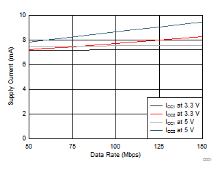
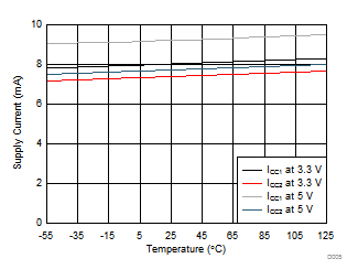
3 V < VCC1, VCC2 < 3.6 V | EN1 = EN2 = 0, OUTx floating, VID ≥ 50 mV | 2.3 | 3.6 | mA | |
| EN1 = EN2 = 0, OUTx floating, VID ≤ –50 mV | 3.5 | 5.6 | |||||
| EN1 = EN2 = 1, RL = 100-Ω differential, VID ≥ 50 mV | 6.2 | 9.9 | |||||
| EN1 = EN2 = 1, RL = 100-Ω differential, VID ≤ –50 mV | 7.5 | 12 | |||||
| EN1 = EN2 = 1, RL = 100-Ω differential, data communication at 50 Mbps |
7.6 | 12.1 | |||||
| EN1 = EN2 = 1, RL = 100-Ω differential, data communication at 125 Mbps |
8.5 | 13.6 | |||||
| EN1 = EN2 = 1, RL = 100-Ω differential, data communication at 150 Mbps |
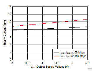
8.9 | 14.2 | |||||
| 4.5 V < VCC1, VCC2 < 5.5 V | EN1 = EN2 = 0, OUTx floating, VID ≥ 50 mV | 2.3 | 3.6 | ||||
| EN1 = EN2 = 0, OUTx floating, VID ≤ –50 mV | 3.6 | 5.7 | |||||
| EN1 = EN2 = 1, RL = 100-Ω differential, VID ≥ 50 mV | 6.6 | 10.5 | |||||
| EN1 = EN2 = 1, RL = 100-Ω differential, VID ≤ –50 mV | 7.9 | 12.6 | |||||
| EN1 = EN2 = 1, RL = 100-Ω differential, data communication at 50 Mbps |
8.3 | 13.2 | |||||
| EN1 = EN2 = 1, RL = 100-Ω differential, data communication at 125 Mbps |
9.7 | 15.5 | |||||
| EN1 = EN2 = 1, RL = 100-Ω differential, data communication at 150 Mbps |
10.3 | 16.4 | |||||
6.11 Timing Requirements for Distortion Correction Scheme
Valid data = 8b10b like data with DC balance and bounded disparity. See Figure 25.| MIN | NOM | MAX | UNIT | ||
|---|---|---|---|---|---|
| tCALIB | Time to complete internal calibration, after exiting idle state. LVDS TX output is held high during this time. During this time valid data must be presented at the receiver. | 250 | 750 | µs | |
| tIDLE | The minimum duration of any idle state that must be maintained between valid data transmissions. | 10 | µs | ||
| tIDLE_OUT | After a channel enters idle state, the internal calibration loses lock after this time, and the LVDS outputs are gated high. | 200 | 600 | ns | |
6.12 Switching Characteristics
(over recommended operating conditions unless otherwise noted)| PARAMETER | TEST CONDITIONS | MIN | TYP | MAX | UNIT | |
|---|---|---|---|---|---|---|
| LVDS CHANNEL | ||||||
| tPLH
tPHL |
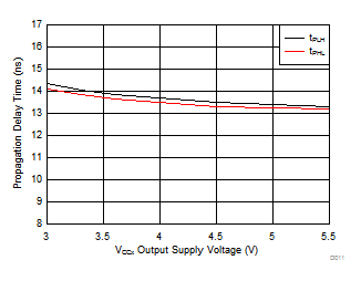
Propagation delay time | 17 | 25 | ns | ||
| tsk(o) | Channel-to-channel output skew time | Opposite directional channels, same voltage and temperature | 4.5 | ns | ||
| tsk(pp) | Part-part skew | Same directional channels, same voltage and temperature | 4.5 | ns | ||
| tCMset | Common-mode setting time after EN = 0 to EN = 1 transition |
Common-mode capacitive load = 100 pF to 0.5 nF |
20 | µs | ||
| Total eye closure | DC balanced data with maximum run length of 6 at 125 Mbps, RX VID = 350 mVPP, 1 ns trf 10%-90%, –40 < TA < 125°C, 3 V < VCC1, VCC2 < 5 V |
30% | ||||
| DC balanced data with maximum run length of 6 at 150 Mbps, RX VID = 350 mVPP, 1 ns trf 10%-90%, –40 < TA < 125°C, 3 V < VCC1, VCC2 < 5 V |
40% | |||||
| tfs | Default output delay time from input power loss | Measured from the time VCC goes below 1.7 V, see Figure 21 | 0.2 | 9 | µs | |
| LVDS TX AND RX | ||||||
| trf | TX differential rise and fall times (20% to 80%) | See Figure 19 | 300 | 780 | 1380 | ps |
| ∆VOC(pp) | TX common-mode voltage peak-to-peak at 100 Mbps | 0 | 150 | mVPP | ||
| tPLZ, tPHZ | TX disable time—valid output to HiZ | See Figure 20 | 10 | 20 | ns | |
| tPZH | TX enable time—HiZ to valid high output(2) | See Figure 20 | 10 | 20 | ns | |
| |VID| | Magnitude of RX input differential voltage for valid operation | Driven with voltage sources on RX pins, see figures in the Parameter Measurement Information section | 100 | 600 | mV | |
| trf(RX) | Allowed RX input differential rise and fall times (20% to 80%) | See Figure 24 | 1 | 0.3 × UI(1) | ns | |
6.13 Insulation Characteristics Curves
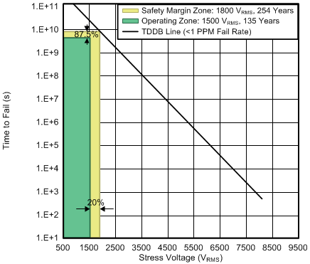
| TA upto 150°C | Operating lifetime = 135 years | |
| Stress-voltage frequency = 60 Hz | ||
| Isolation working voltage = 1500 VRMS | ||
 Figure 3. Thermal Derating Curve for Limiting Current for DW Package
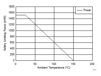 Figure 5. Thermal Derating Curve for Limiting Power for DW Package
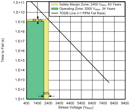
| TA upto 150°C | Operating lifetime = 34 years | |
| Stress-voltage frequency = 60 Hz | ||
| Isolation working voltage = 2000 VRMS | ||
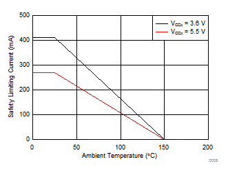 Figure 4. Thermal Derating Curve for Limiting Current for DWW Package
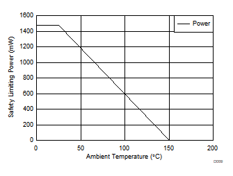 Figure 6. Thermal Derating Curve for Limiting Power for DWW Package
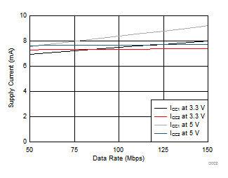
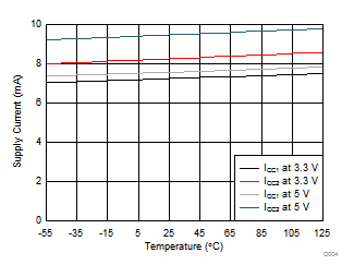
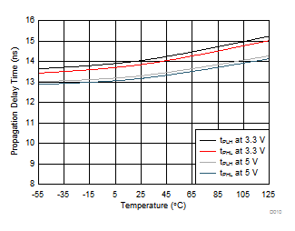
6.14 Typical Characteristics
| TA = 25°C | CH-A toggle |
| TA = 25°C |
| Data rate = 150 Mbps | CH-B toggle |
| TA = 25°C |
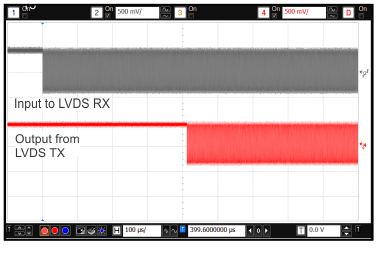 Figure 15. Distortion Correction Scheme Calibration Time (tCALIB)
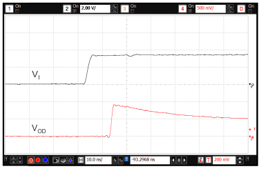 Figure 17. Disable to Enable Time (tPZH)
| TA = 25°C | CH-B toggle |
| Data rate = 150 Mbps | CH-A toggle |
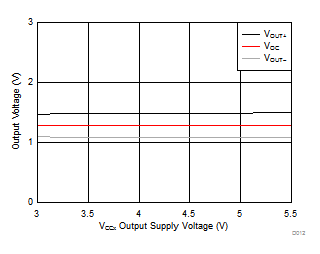
| TA = 25°C |
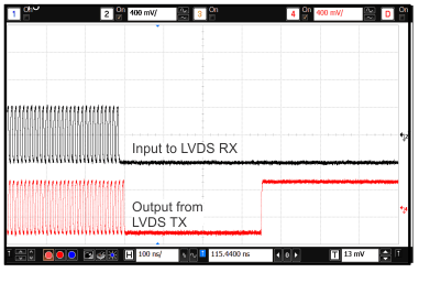 Figure 16. Transition From Valid Data to Idle (tIDLE_OUT)
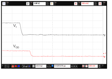 Figure 18. Disable Time (tPLZ, tPHZ)
7 Parameter Measurement Information

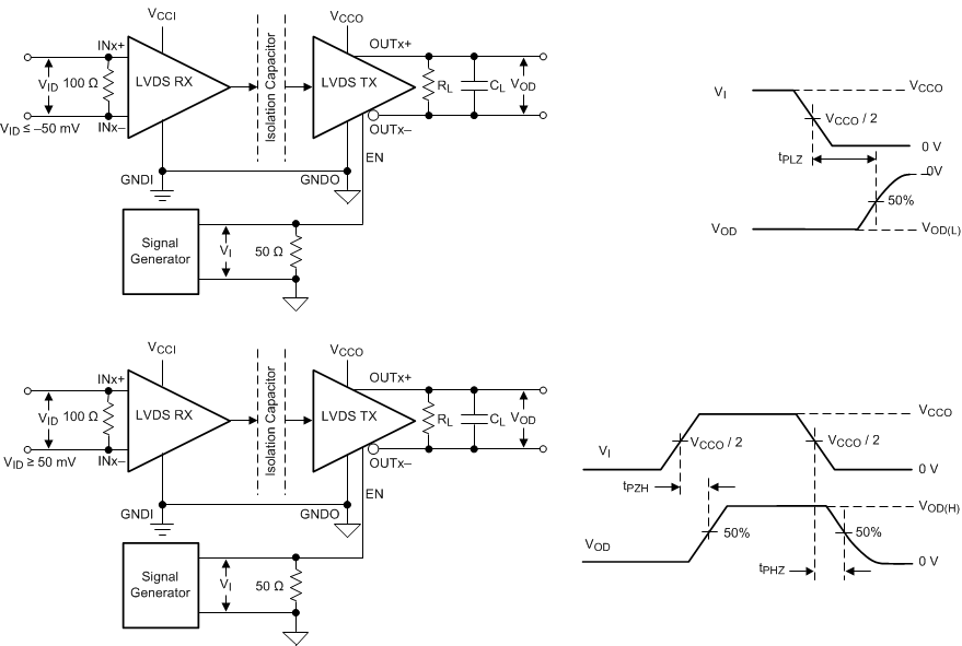
tr ≤ 3 ns, tf ≤ 3 ns, ZO = 50 Ω.

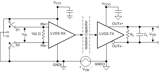
 Figure 23. Driver Test Circuit
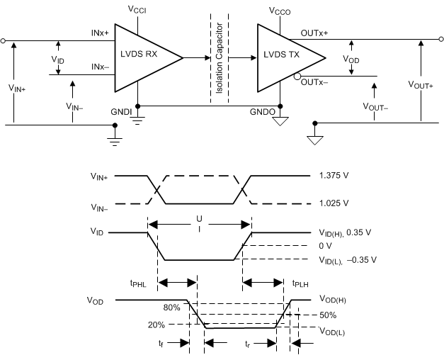 Figure 24. Voltage Definitions and Waveforms
8 Detailed Description
8.1 Overview
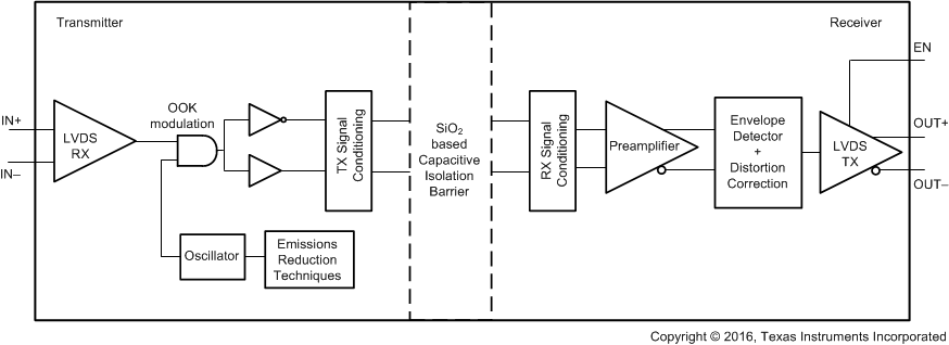
The ISO7821LLS device is an isolated LVDS buffer. The differential signal received on the LVDS input pins is first converted to CMOS logic levels. It is then transmitted across a silicon dioxide based capacitive isolation barrier using an On-Off Keying (OOK) modulation scheme. A high frequency carrier transmitted across the barrier represents one logic state and an absence of a carrier represents the other logic state. On the other side of the barrier a demodulator converts the OOK signal back to logic levels, which is then converted to LVDS outputs by a differential driver. This device incorporates advanced circuit techniques to maximize CMTI performance and minimize radiated emissions.
The ISO7821LLS device implements an eye-diagram improvement scheme to correct for signal distortions that are introduced in the LVDS receiver as well as the isolation channel. This enables the device to guarantee an eye closure of less than 30% at 125 Mbps, and less than 40% at 150 Mbps. The distortion correction scheme is optimized for operation with DC balanced data (for example 8b10b or equivalent) with a maximum run length of 6. The minimum data-rate of operation is also constrained to 50 Mbps. For general purpose data communication from 0 to 100 Mbps, the ISO782xLL family of devices should be considered.
The ISO7821LLS device is TIA/EIA-644-A standard compliant. The LVDS transmitter drives a minimum differential-output voltage magnitude of 250 mV into a 100-Ω load, and the LVDS receiver is capable of detecting differential signal ≥50 mV in magnitude. The device consumes 11 mA per channel at 150 Mbps with 5-V supplies.
The Functional Block Diagram section shows a conceptual block diagram of one channel of the ISO7821LLS device.
8.2 Functional Block Diagram
8.3 Feature Description
The ISO7821LLS device is available in a two-channel configuration with a default differential-high output state. Table 1 lists the device features.
Table 1. Device Features
| PART NUMBER | CHANNEL DIRECTION | RATED ISOLATION | MAXIMUM DATA RATE | DEFAULT DIFFERENTIAL OUTPUT |
|---|---|---|---|---|
| ISO7821LLS | 1 Forward, 1 Reverse | 5700 VRMS / 8000 VPK (1) | 150 Mbps | High |
8.3.1 Distortion-Correction Scheme
The ISO7821LLS device implements a distortion-correction scheme to correct for signal distortions that are introduced in the LVDS receiver as well as the isolation channel. This scheme is optimized for a DC-balanced data-stream with a maximum run length of 6. One example of such a data stream is 8b10b encoded data. The minimum data rate supported by the ISO7821LLS device is 50 Mbps and the maximum is 150 Mbps.
Figure 25 shows the timing requirements associated with the distortion correction scheme (see the Timing Requirements for Distortion Correction Scheme table for timing parameters). The input to the LVDS channel should be either idle low, idle high, or should have clock or DC-balanced data transitions at 25 MHz / 50 Mbps or higher. Low frequency or DC-unbalanced data is not allowed. The distortion-correction scheme runs an internal calibration each time the LVDS channel transitions from an idle state to a data transmission state. The calibration runs for a period of tCALIB during which the LVDS channel output is held at logic high. This calibration is also run at power up. Lack of activity on the receive inputs for a period greater than tIDLE_OUT takes the channel to an uncalibrated state. If the communication protocol requires the channel to transition to the idle state, the idle-high or idle-low state must be held for at least duration of tIDLE.

Logic high → VIN+ > VIN–
Logic low → VIN– > VIN+
Valid data = 8b10b like data with DC balance and bounded disparity.
8.4 Device Functional Modes
Table 2 lists the functional modes for the ISO7821LLS device.
Table 2. ISO7821LLS Function Table(1)
| VCCI | VCCO | INPUT (INx±)(2) |
OUTPUT ENABLE (ENx) |
OUTPUT (OUTx±)(3) |
COMMENTS |
|---|---|---|---|---|---|
| PU | PU | H | H or open | H | Normal Operation: A channel output assumes the logic state of the input. |
| L | H or open | L | |||
| I | H or open | H or L | |||
| X | PU | X | L | Z | A low-logic state at the output enable causes the outputs to be in high impedance. |
| PD | PU | X | H or open | H | Default mode: When VCCI is unpowered, a channel output assumes the logic high state. When VCCI transitions from unpowered to powered up, a channel output assumes the logic state of the input. When VCCI transitions from powered up to unpowered, a channel output assumes the selected default high state. |
| X | PD | X | X | Undetermined | When VCCO is unpowered, a channel output is undetermined. When VCCO transitions from unpowered to powered up, a channel output assumes the logic state of the input |
8.4.1 Device I/O Schematics
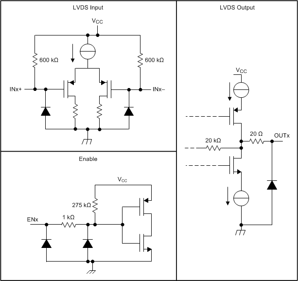 Figure 26. Device I/O Schematics
9 Application and Implementation
NOTE
Information in the following applications sections is not part of the TI component specification, and TI does not warrant its accuracy or completeness. TI’s customers are responsible for determining suitability of components for their purposes. Customers should validate and test their design implementation to confirm system functionality.
9.1 Application Information
The ISO7821LLS device is a high-performance, reinforced isolated dual-LVDS buffer. Isolation can be used to help achieve human and system safety, to overcome ground potential difference (GPD), or to improve noise immunity and system performance.
The LVDS signaling can be used over most interfaces to achieve higher data rates because the LVDS is only a physical layer. LVDS can also be used for a proprietary communication scheme implemented between a host controller and a slave. Example use cases include connecting a high-speed I/O module to a host controller, a subsystem connecting to a backplane, and connection between two high-speed subsystems. Many of these systems operate under harsh environments making them susceptible to electromagnetic interferences, voltage surges, electrical fast transients (EFT), and other disturbances. These systems must also meet strict limits on radiated emissions. Using isolation in combination with a robust low-noise signaling standard such as LVDS, achieves both high immunity to noise and low emissions.
Example end applications that could benefit from the ISO7821LLS device include high-voltage motor control, test and measurement, industrial automation, and medical equipment.
9.2 Typical Application
One application for isolated LVDS buffers is for point-to-point communication between two high-speed capable, application-specific integrated circuits (ASICs) or FPGAs. In a high-voltage motor control application, for example, Node 1 could be a controller on a low-voltage or earth referenced board, and Node 2, could be controller placed on the power board, biased to high voltage. Figure 27 and Figure 28 show the application schematics.
Figure 28 provides further details of using the ISO7821LLS device to isolate the LVDS interface. The LVDS connection to the ISO7821LLS device can be traces on a board (shown as straight lines between Node 1 and the ISO7821LLS device), a twisted pair cable (as shown between Node 2 and the ISO7821LLS device), or any other controlled impedance channel. Differential 100-Ω terminations are placed near each LVDS receiver. The characteristic impedance of the channel should also be 100-Ω differential.
In the example shown in Figure 27 and Figure 28, the ISO7821LLS device provides reinforced or safety isolation between the high-voltage elements of the motor drive and the low-voltage control circuitry. This configuration also ensures reliable communication, regardless of the high conducted and radiated noise present in the system.
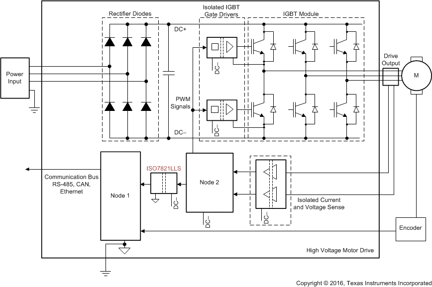 Figure 27. Isolated LVDS Interface in Motor Control Application
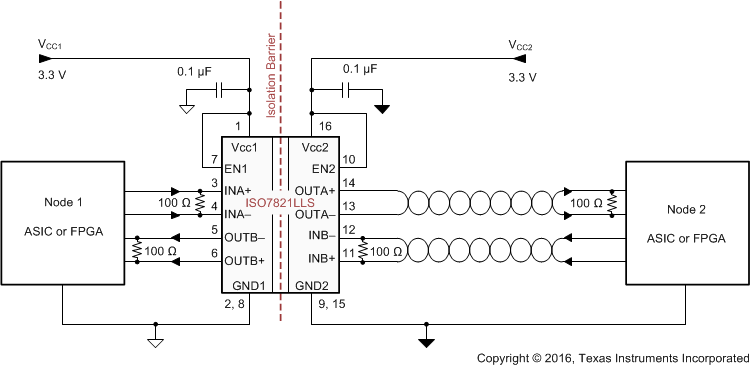 Figure 28. Isolated LVDS Interface Between Two Nodes (ASIC or FPGA)
9.2.1 Design Requirements
For the ISO7821LLS device, use the parameters listed in Table 3.
Table 3. Design Parameters
| PARAMETER | VALUE |
|---|---|
| Supply voltage range, VCC1 and VCC2 | 3 V to 5.5 V |
| Receiver common-mode voltage range | 0.5 |VID| to 2.4 – 0.5 |VID| |
| External termination resistance | 100 Ω |
| Interconnect differential characteristic impedance | 100 Ω |
| Signaling rate | 50 to 150 Mbps |
| Decoupling capacitor from VCC1 and GND1 | 0.1 µF |
| Decoupling capacitor from VCC2 and GND2 | 0.1 µF |
9.2.2 Detailed Design Procedure
The ISO7821LLS device has minimum requirements on external components for correct operation. External bypass capacitors (0.1 µF) are required for both supplies (VCC1 and VCC2). A termination resistor with a value of 100 Ω is required between each differential input pair (INx+ and INx–), with the resistors placed as close to the device pins as possible. A differential termination resistor with a value of 100 Ω is required on the far end for the LVDS transmitters. Figure 29 shows these connections.
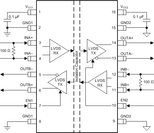 Figure 29. Typical ISO7821LLS Circuit Hook-Up
9.2.2.1 Electromagnetic Compatibility (EMC) Considerations
Many applications in harsh industrial environment are sensitive to disturbances such as electrostatic discharge (ESD), electrical fast transient (EFT), surge and electromagnetic emissions. These electromagnetic disturbances are regulated by international standards such as IEC 61000-4-x and CISPR 22. Although system-level performance and reliability depends, to a large extent, on the application board design and layout, the ISO7821LLS device incorporates many chip-level design improvements for overall system robustness. Some of these improvements include:
- Robust ESD protection cells for input and output signal pins and inter-chip bond pads.
- Low-resistance connectivity of ESD cells to supply and ground pins.
- Enhanced performance of high voltage isolation capacitor for better tolerance of ESD, EFT and surge events.
- Bigger on-chip decoupling capacitors to bypass undesirable high energy signals through a low impedance path.
- PMOS and NMOS devices isolated from each other by using guard rings to avoid triggering of parasitic SCRs.
- Reduced common mode currents across the isolation barrier by ensuring purely differential internal operation.
9.2.3 Application Curve
Figure 30 shows a typical eye diagram of the ISO7821LLS device which indicates low jitter and a wide-open eye at the maximum data rate of 150 Mbps.
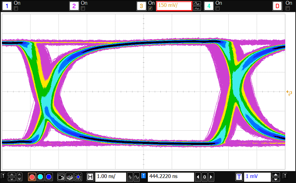 Figure 30. Eye Diagram at 150 Mbps PRBS, 3.3 V and 25°C
10 Power Supply Recommendations
To help ensure reliable operation at data rates and supply voltages, a 0.1-μF bypass capacitor is recommended at the input and output supply pins (VCC1 and VCC2). The capacitors should be placed as close to the supply pins as possible. If only a single primary-side power supply is available in an application, isolated power can be generated for the secondary-side with the help of a transformer driver such as Texas Instruments' SN6501 or SN6505. For such applications, detailed power supply design and transformer selection recommendations are available in the following data sheets: SN6501 Transformer Driver for Isolated Power Supplies (SLLSEA0) and SN6505 Low-Noise 1-A Transformer Drivers for Isolated Power Supplies (SLLSEP9).
11 Layout
11.1 Layout Guidelines
A minimum of four layers is required to accomplish a low EMI PCB design (see Figure 31). Layer stacking should be in the following order (top-to-bottom): high-speed signal layer, ground plane, power plane and low-frequency signal layer.
- Routing the high-speed traces on the top layer avoids the use of vias (and the introduction of their inductances) and allows for clean interconnects between the isolator and the transmitter and receiver circuits of the data link.
- Placing a solid ground plane next to the high-speed signal layer establishes controlled impedance for transmission line interconnects and provides an excellent low-inductance path for the return current flow.
- Placing the power plane next to the ground plane creates additional high-frequency bypass capacitance of approximately 100 pF/in2.
- Routing the slower speed control signals on the bottom layer allows for greater flexibility as these signal links usually have margin to tolerate discontinuities such as vias.
- While routing differential traces on a board, TI recommends that the distance between two differential pairs be much higher (at least 2x) than the distance between the traces in a differential pair. This distance minimizes crosstalk between the two differential pairs.
If an additional supply voltage plane or signal layer is needed, add a second power or ground plane system to the stack to keep it symmetrical. This makes the stack mechanically stable and prevents it from warping. Also the power and ground plane of each power system can be placed closer together, thus increasing the high-frequency bypass capacitance significantly.
The ISO7821LLS device requires no special layout considerations to mitigate electromagnetic emissions.
For detailed layout recommendations, see the application note, Digital Isolator Design Guide (SLLA284).
11.1.1 PCB Material
For digital circuit boards operating at less than 150 Mbps (or rise and fall times higher than 1 ns) and trace lengths of up to 10 inches, use standard FR–4 UL94V-0 epoxy-glass as PCB material. This PCB is preferred over cheaper alternatives because of lower dielectric losses at high frequencies, less moisture absorption, greater strength and stiffness, and self-extinguishing flammability-characteristics.
11.2 Layout Example
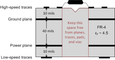 Figure 31. Layout Example
12 Device and Documentation Support
12.1 Documentation Support
12.1.1 Related Documentation
For related documentation see the following:
- Digital Isolator Design Guide (SLLA284)
- ISO782xLLx Isolated Dual LVDS Buffer Evaluation Module (SLLU240)
- Isolation Glossary (SLLA353)
- LVDS Owner’s Manual (SNLA187)
- SN6501 Transformer Driver for Isolated Power Supplies (SLLSEA0)
- SN6505 Low-Noise 1-A Transformer Drivers for Isolated Power Supplies (SLLSEP9)
12.2 Receiving Notification of Documentation Updates
To receive notification of documentation updates — go to the product folder for your device on ti.com. In the upper right-hand corner, click the Alert me button to register and receive a weekly digest of product information that has changed (if any). For change details, check the revision history of any revised document.
12.3 Community Resources
The following links connect to TI community resources. Linked contents are provided "AS IS" by the respective contributors. They do not constitute TI specifications and do not necessarily reflect TI's views; see TI's Terms of Use.
-
TI E2E™ Online Community TI's Engineer-to-Engineer (E2E) Community. Created to foster collaboration among engineers. At e2e.ti.com, you can ask questions, share knowledge, explore ideas and help solve problems with fellow engineers.
-
Design Support TI's Design Support Quickly find helpful E2E forums along with design support tools and contact information for technical support.
12.4 Trademarks
E2E is a trademark of Texas Instruments.
All other trademarks are the property of their respective owners.
12.5 Electrostatic Discharge Caution

This integrated circuit can be damaged by ESD. Texas Instruments recommends that all integrated circuits be handled with appropriate precautions. Failure to observe proper handling and installation procedures can cause damage.
ESD damage can range from subtle performance degradation to complete device failure. Precision integrated circuits may be more susceptible to damage because very small parametric changes could cause the device not to meet its published specifications.
12.6 Glossary
SLYZ022 — TI Glossary.
This glossary lists and explains terms, acronyms, and definitions.
13 Mechanical, Packaging, and Orderable Information
The following pages include mechanical, packaging, and orderable information. This information is the most current data available for the designated devices. This data is subject to change without notice and revision of this document. For browser-based versions of this data sheet, refer to the left-hand navigation.
IMPORTANT NOTICE
Texas Instruments Incorporated and its subsidiaries (TI) reserve the right to make corrections, enhancements, improvements and other changes to its semiconductor products and services per JESD46, latest issue, and to discontinue any product or service per JESD48, latest issue. Buyers should obtain the latest relevant information before placing orders and should verify that such information is current and complete. All semiconductor products (also referred to herein as "components") are sold subject to TI's terms and conditions of sale supplied at the time of order acknowledgment.
TI warrants performance of its components to the specifications applicable at the time of sale, in accordance with the warranty in TI's terms and conditions of sale of semiconductor products. Testing and other quality control techniques are used to the extent TI deems necessary to support this warranty. Except where mandated by applicable law, testing of all parameters of each component is not necessarily performed.
TI assumes no liability for applications assistance or the design of Buyers' products. Buyers are responsible for their products and applications using TI components. To minimize the risks associated with Buyers' products and applications, Buyers should provide adequate design and operating safeguards.
TI does not warrant or represent that any license, either express or implied, is granted under any patent right, copyright, mask work right, or other intellectual property right relating to any combination, machine, or process in which TI components or services are used. Information published by TI regarding third-party products or services does not constitute a license to use such products or services or a warranty or endorsement thereof. Use of such information may require a license from a third party under the patents or other intellectual property of the third party, or a license from TI under the patents or other intellectual property of TI.
Reproduction of significant portions of TI information in TI data books or data sheets is permissible only if reproduction is without alteration and is accompanied by all associated warranties, conditions, limitations, and notices. TI is not responsible or liable for such altered documentation. Information of third parties may be subject to additional restrictions.
Resale of TI components or services with statements different from or beyond the parameters stated by TI for that component or service voids all express and any implied warranties for the associated TI component or service and is an unfair and deceptive business practice. TI is not responsible or liable for any such statements.
Buyer acknowledges and agrees that it is solely responsible for compliance with all legal, regulatory and safety-related requirements concerning its products, and any use of TI components in its applications, notwithstanding any applications-related information or support that may be provided by TI. Buyer represents and agrees that it has all the necessary expertise to create and implement safeguards which anticipate dangerous consequences of failures, monitor failures and their consequences, lessen the likelihood of failures that might cause harm and take appropriate remedial actions. Buyer will fully indemnify TI and its representatives against any damages arising out of the use of any TI components in safety-critical applications.
In some cases, TI components may be promoted specifically to facilitate safety-related applications. With such components, TI's goal is to help enable customers to design and create their own end-product solutions that meet applicable functional safety standards and requirements. Nonetheless, such components are subject to these terms.
No TI components are authorized for use in FDA Class III (or similar life-critical medical equipment) unless authorized officers of the parties have executed a special agreement specifically governing such use.
Only those TI components which TI has specifically designated as military grade or "enhanced plastic" are designed and intended for use in military/aerospace applications or environments. Buyer acknowledges and agrees that any military or aerospace use of TI components which have not been so designated is solely at the Buyer's risk, and that Buyer is solely responsible for compliance with all legal and regulatory requirements in connection with such use.
TI has specifically designated certain components as meeting ISO/TS16949 requirements, mainly for automotive use. In any case of use of non-designated products, TI will not be responsible for any failure to meet ISO/TS16949.
Products
- Audio: www.ti.com/audio
- Amplifiers: amplifier.ti.com
- Data Converters: dataconverter.ti.com
- DLP® Products: www.dlp.com
- DSP: dsp.ti.com
- Clocks and Timers: www.ti.com/clocks
- Interface: interface.ti.com
- Logic: logic.ti.com
- Power Mgmt: power.ti.com
- Microcontrollers: microcontroller.ti.com
- RFID: www.ti.rfid.com
- OMAP Application Processors: www.ti.com/omap
- Wireless Connectivity: www.ti.com/wirelessconnectivity
Applications
- Automotive and Transportation: www.ti.com/automotive
- Communications and Telecom: www.ti.com/communications
- Computers and Peripherals: www.ti.com/computers
- Consumer Electronics: www.ti.com/consumer-apps
- Energy and Lighting: www.ti.com/energy
- Industrial: www.ti.com/industrial
- Medical: www.ti.com/medical
- Security: www.ti.com/security
- Space, Avionics and Defense: www.ti.com/space-avionics-defense
- Video & Imaging: www.ti.com/video
TI E2E Community : e2e.ti.com
Mailing Address: Texas Instruments, Post Office Box 655303, Dallas, Texas 75265
Copyright© 2016, Texas Instruments Incorporated