SLUS515G September 2002 – December 2015
PRODUCTION DATA.
- 1 Features
- 2 Applications
- 3 Description
- 4 Revision History
- 5 Pin Configuration and Functions
- 6 Specifications
- 7 Detailed Description
- 8 Application and Implementation
- 9 Power Supply Recommendations
- 10Layout
- 11Device and Documentation Support
- 12Mechanical, Packaging, and Orderable Information
1 Features
- Transition Mode PFC Controller for Low Implementation Cost
- Industry Pin Compatibility With Improved Feature Set
- Improved Transient Response With Slew-Rate Comparator
- Zero Power Detect to Prevent Overvoltage Protection (OVP) During Light Load Conditions
- Accurate Internal VREF for Tight Output Regulation
- Two UVLO Options
- OVP, Open-Feedback Protection, and Enable Circuits
- ±750-mA Peak Gate Drive Current
- Low Start-Up and Operating Currents
- Lead (Pb)-Free Packages
2 Applications
- Single-Stage PFC Flyback Converters for Lighting and Motor Drives
- Switch-Mode Power Supplies for Desktops, Monitors, TVs, and Set Top Boxes (STBs)
- AC Adapter Front-End Power Supplies
- Electronic Ballasts
3 Description
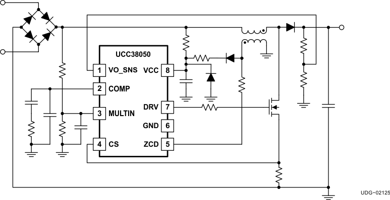
The UCC38050 and UCC38051 are PFC controllers for low-to-medium power applications requiring compliance with IEC 1000-3-2 harmonic reduction standard. The controllers are designed for a boost preregulator operating in transition mode (also referred to as boundary-conduction mode or critical conduction-mode operation). They feature a transconductance voltage amplifier for feedback error processing, a simple multiplier for generating a current command proportional to the input voltage, a current-sense (PWM) comparator, PWM logic, and a totem-pole driver for driving an external FET.
In the transition mode operation, the PWM circuit is self-oscillating, with the turnon being governed by an inductor zero-current detector (ZCD pin), and the turnoff being governed by the current-sense comparator. Additionally, the controller provides features such as peak current limit, default timer, overvoltage protection (OVP) and enable.
Device Information(1)
| PART NUMBER | PACKAGE | BODY SIZE (NOM) |
|---|---|---|
| UCC28050, UCC28051, UCC38050, UCC38051 | SOIC (8) | 3.91 mm × 4.90 mm |
| PDIP (8) | 6.35 mm × 9.81 mm |
- For all available packages, see the orderable addendum at the end of the data sheet.
Simplified Application Diagram
