SLVS762C June 2007 – July 2015 TPS62242
PRODUCTION DATA.
- 1 Features
- 2 Applications
- 3 Description
- 4 Revision History
- 5 Device Options
- 6 Pin Configuration and Functions
- 7 Specifications
- 8 Detailed Description
- 9 Application and Implementation
- 10Power Supply Recommendations
- 11Layout
- 12Device and Documentation Support
- 13Mechanical, Packaging, and Orderable Information
1 Features
- High Efficiency - Greater Than 94%
- Output Current up to 300 mA
- VIN Range from 2 V to 6 V for Li-ion Batteries With Extended Voltage Range
- 2.25-MHz Fixed-Frequency Operation
- Power Save Mode at Light Load Currents
- Output Voltage Accuracy in PWM Mode ±1.5%
- Adjustable Output Voltage from 0.6 V to VIN
- Typical 15-μA Quiescent Current
- 100% Duty Cycle for Lowest Dropout
- Available in a SOT (5) and 2-mm × 2-mm × 0.8-mm WSON (6) Package
- Allows <1-mm Solution Height
2 Applications
- Bluetooth™ Headsets
- Mobile Phones, Smart Phones
- WLAN
- Low Power DSP Supplies
- Portable Media Players
- Digital Cameras
3 Description
The TPS6224x device is a highly efficient synchronous step-down DC-DC converter. The device provides up to 300-mA output current from a single Li-Ion cell and is ideal for battery powered portable applications like mobile phones and other portable equipment.
With an wide input voltage range of 2 V to 6 V, the device also supports two- and three-cell alkaline, 3.3-V and 5-V input voltage rails.
The TPS6224x operates at 2.25-MHz fixed switching frequency and enters power save mode operation at light load currents to maintain high efficiency over the entire load current range.
The power save mode is optimized for low output voltage ripple. For low-noise applications, the device can be forced into fixed-frequency pulse width modulation (PWM) mode by pulling the MODE pin high. In shutdown mode, the current consumption is reduced to less than 1 μA. The TPS6224x allows the use of small inductors and capacitors to achieve a small solution size.
The TPS6224x operates over a free-air temperature range of –40°C to 85°C. The device is available in a 5-pin SOT and a 6-pin 2-mm × 2-mm WSON package.
Device Information(1)
| PART NUMBER | PACKAGE | BODY SIZE (NOM) |
|---|---|---|
| TPS6224x | WSON (6) | 2.00 mm × 2.00 mm |
| SOT (5) | 2.90 mm × 1.60 mm |
- For all available packages, see the orderable addendum at the end of the data sheet.
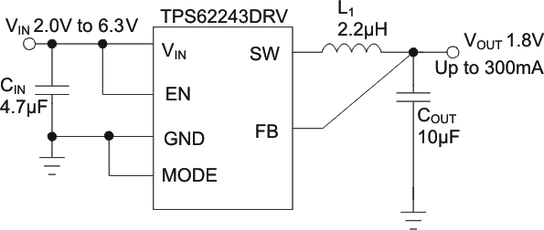
Typical Application Schematic

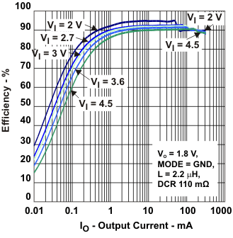
Efficiency vs Output Current
