-
How GaN Improves Solar Charge Controllers
How GaN Improves Solar Charge Controllers
This application brief describes how TI GaN device improves solar charge controller. Using TI GaN device improves efficiency and reduces PCB size without increasing BOM cost compared with MOSFET.
With the rapid development of electronic and electrical devices, the power required from these devices becomes much bigger than ever before. Solar energy becomes a good choice for many families to either reduce electrical bills or turning to a greener future, and semiconductors play an important role.
A compact and highly efficient power converter for solar application can both save user’s area in house and money. Gallium nitride (GaN) makes this trend possible. TI’s new mid-voltage GaN designs make the design much easier by integrating the driver and optimizing the power loop.
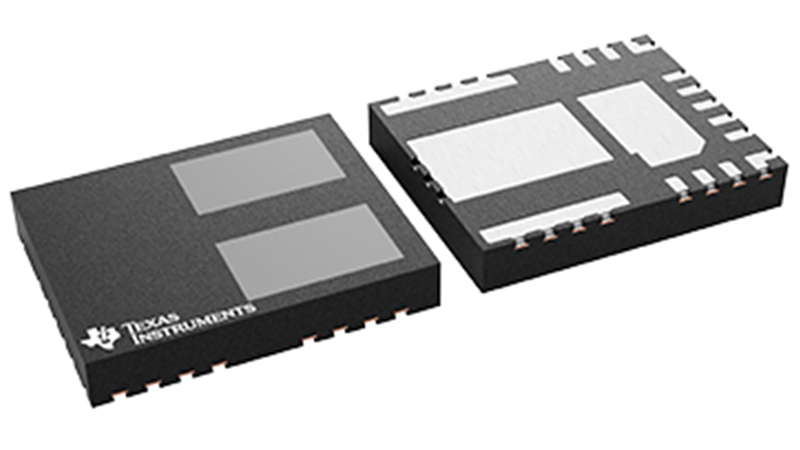 Figure 1 TI LMG2100
A solar charge controller works with photovoltaic (PV) array, use maximum power point tracking (MPPT) algorithm to generate power for batteries and electrical loads in off-grid and hybrid off-grid applications. The output voltage and output current are regulated. A controller can safely regulate the battery to prevent over-charge or over-discharge to extend the lifetime of a battery. A highly efficient power converter inside the solar charge controller can maximize the power yield from the sunlight.
 Figure 2 Solar Charge Controller Diagram
TIDA-010042 reference design is a solar charge controller which operates from 15V to 60V input voltage, 12V, 24V batteries, and can deliver more than 400W power. In the old design, which contains a two-phase interleaved buck converter, CSD19531Q5A was selected as the main power switch MOSFET, switching at 180kHz each phase.
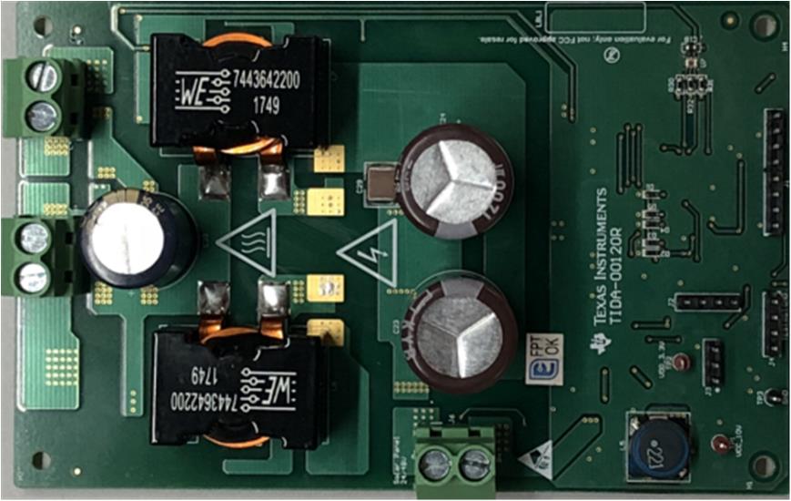
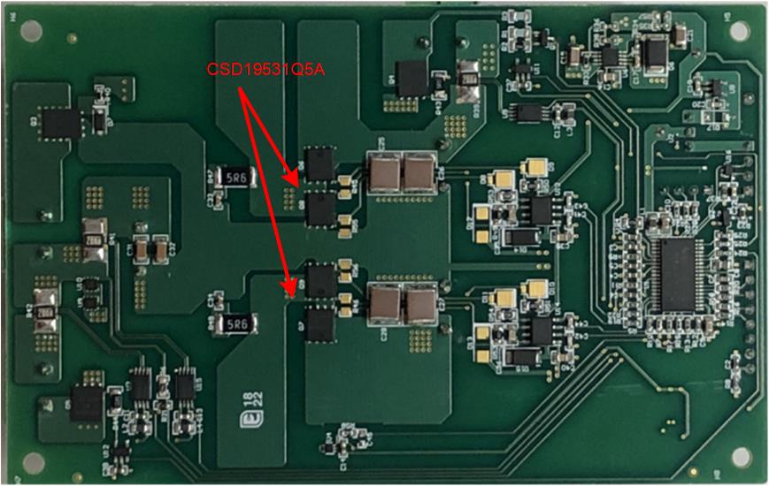 Figure 3 Old TIDA-010042 Board
When the board was tested under 12V and 24V load condition, with a fixed duty cycle of 0.6. With 12V load, peak efficiency is 96.7%, European weighted efficiency is about 96.4%. With 24V load, peak efficiency is 97.3%, European weighted efficiency is about 96.4%.
 Figure 4 Old TIDA-010042 Efficiency Curve
GaN device allows higher switching frequency at same or lower losses, by changing MOSFET to TI’s new mid-voltage GaN device LMG2100, which has lower Rds(on) and much lower parasitic capacitance. A converter with higher switching frequency can make the passive components smaller, thus to decrease the PCB size, and reduce cost. Also, higher efficiency reduces the thermal dissipation and outputs more power with the same solar panel, saves heat dissipation material and electrical bill.
The new TIDA-010042 uses LMG2100 as a single-phase buck converter power stage, simplifies design requirements. By introducing LMG2100, PCB area saves about 37%, and BOM cost goes down 37% as well.
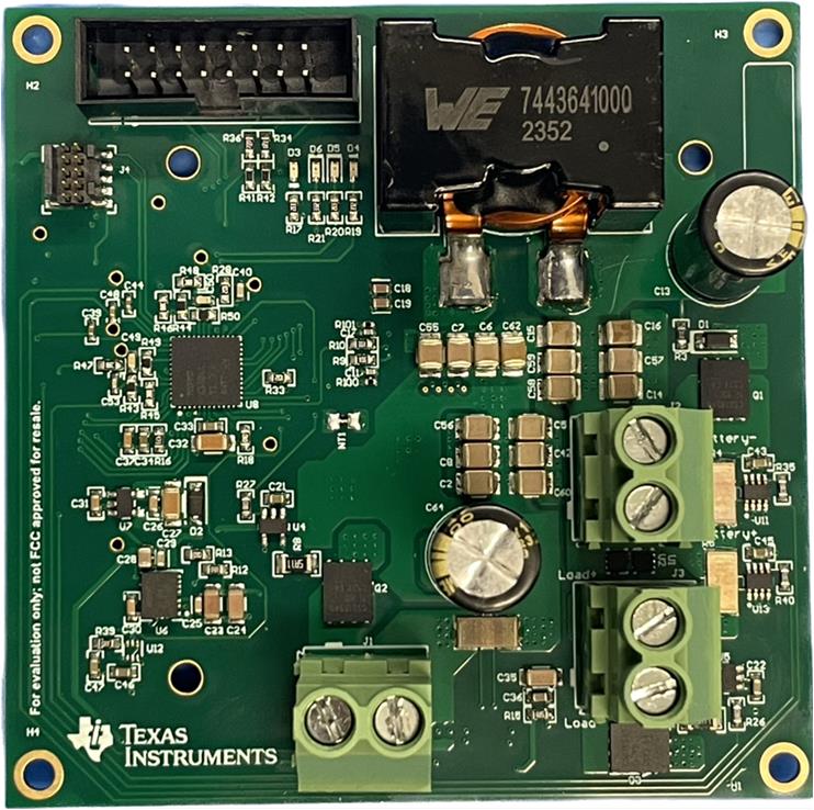
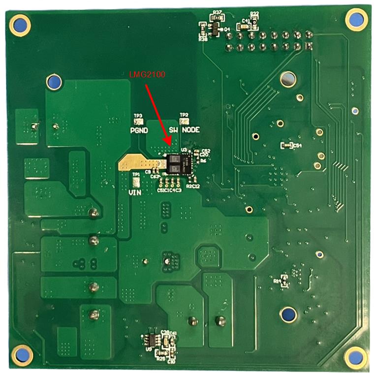 Figure 5 New TIDA-010042 Board
Tested under the same condition with TIDA-010042 using MOSFET, using GaN with 2-layer PCB, switching at 250kHz, peak efficiency with 12V load and 24V load is 98.4% and 98.5%, respectively. European weighted efficiency is 97.5% and 98.2%, respectively. Compared with MOSFET version, peak efficiency improves at least by 1.2%, European weighted efficiency improved at least by 1.1%, while the BOM cost further decreases.
 Figure 6 New TIDA-010042 Efficiency
To fully leverage the capability of GaN device, TI recommends to use at least 4-layer PCB, due to high turn-on and turn-off speed, it requires very low input loop inductance of Buck Converter. 4-layer PCB can help minimize the input loop inductance by optimize the layout without increasing cost much since the board is very small. With 2 additional layer, PCB losses and switching losses reduced a lot, with further increased efficiency. European weighted efficiency under 12V and 24V load is 97.9% and 98.5%, respectively, improved about 0.3% compared with 2-layer version. Figure 7 shows the efficiency comparison between solar charge controller using TI GaN and MOSFET, which shows a great performance improvement.
 Figure 7 Test with 12V Load
System
 Figure 8 Test with 24V Load
System
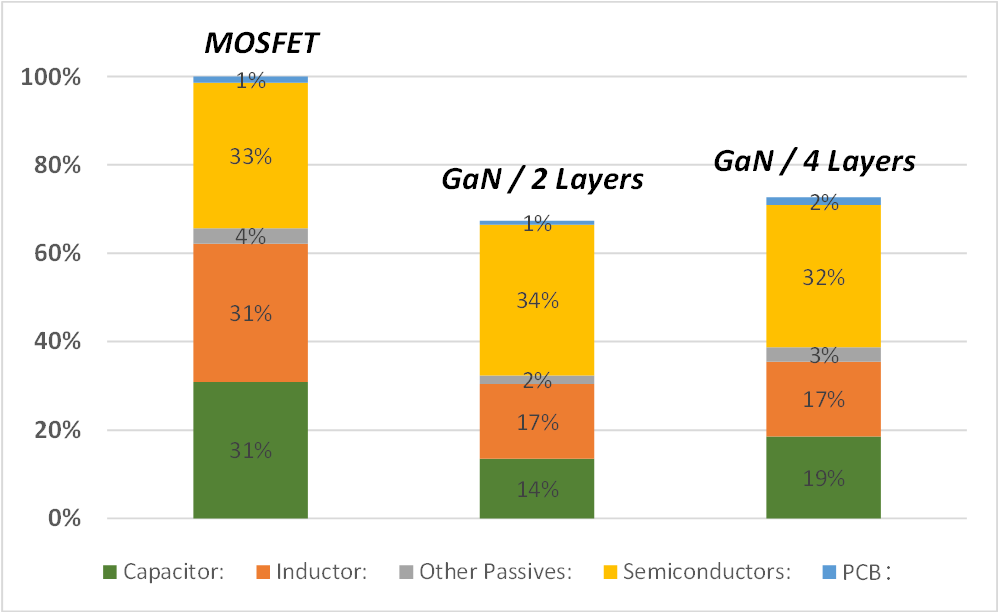 Figure 9 BOM Cost Comparison
Figure 9 shows the BOM cost comparison. The old version uses interleaved buck with MOSFET, which require more passive components driving cost and size up. Main saving are coming from inductor and passive components. In addition, with 4 layer-board, the GaN device can dissipate all the heat into PCB in 400W condition without adding fan or heatsink, the junction temperature is well below the safety working zone. Savings on cooling material have not been considered in Figure 9.