FPGA Power Made Simple: System Architecture
Callie Wallace
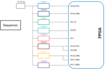
Field-programmable gate arrays (FPGAs) are used in applications ranging from medical devices, to wire communications, to aerospace and defense. FPGAs simplify the design process by providing a reprogrammable circuit; this ability to repeatedly reprogram enables quick prototyping and eliminates the need to create a custom application-specific integrated circuit (ASIC). FPGAs are a relatively inexpensive solution even in small quantities, making them popular at both small and large companies. However, because of the multiple rails required to power the FPGA (as shown in Figure 1), it can be confusing to design the power circuitry.
 Figure 1 Basic FPGA Schematic
Each rail will have different requirements for current, accuracy, voltage ripple, load transients and sequencing. This means that the power design will require multiple power supplies to meet all of the different rail requirements. In this four-part series, I will break down the basic design considerations of designing FPGA power circuitry, starting with my first topic: system architecture.
The requirements of your application will inform your system architecture. Typically, as shown in Figure 2, designers will use a DC/DC converter to step down from the power source to an intermediate rail. Additional power supplies will then step the intermediate voltage down to the point-of-load (POL) power required.
 Figure 2 Typical System
Architectures
Figure 2 Typical System
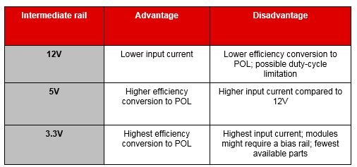
ArchitecturesOne of the first steps is deciding what voltage to use for the intermediate rail. The most common intermediate rail voltages are 12V, 5V and 3.3V. Typically, the lower the intermediate rail, the higher the efficiency of the voltage conversion to the POL power level. However, a lower intermediate rail voltage will require a higher input current. There are also fewer devices available that can step down to 3.3V, depending on how high the voltage of the power source is. Table 1 summarizes the trade-offs.

|
Defining the system architecture will determine what devices and how much power you need to feed your design. After selecting the architecture, you can then move on to the next step: determining the current level. To determine the current requirements, I recommend that you use the spreadsheets provided by your FPGA vendor. From these spreadsheets, input the specific FPGA you are using and other details of your design (like clock frequency and temperature) and it will calculate the voltage and current requirements of each rail.
Once you define the system architecture and have estimated the current requirements, it is time to start looking at the requirements of individual rails which will be covered in the next blog post. In the meantime, get more information on TI’s solutions for Xilinx and Altera FPGAs.
IMPORTANT NOTICE AND DISCLAIMER
TI PROVIDES TECHNICAL AND RELIABILITY DATA (INCLUDING DATASHEETS), DESIGN RESOURCES (INCLUDING REFERENCE DESIGNS), APPLICATION OR OTHER DESIGN ADVICE, WEB TOOLS, SAFETY INFORMATION, AND OTHER RESOURCES “AS IS” AND WITH ALL FAULTS, AND DISCLAIMS ALL WARRANTIES, EXPRESS AND IMPLIED, INCLUDING WITHOUT LIMITATION ANY IMPLIED WARRANTIES OF MERCHANTABILITY, FITNESS FOR A PARTICULAR PURPOSE OR NON-INFRINGEMENT OF THIRD PARTY INTELLECTUAL PROPERTY RIGHTS.
These resources are intended for skilled developers designing with TI products. You are solely responsible for (1) selecting the appropriate TI products for your application, (2) designing, validating and testing your application, and (3) ensuring your application meets applicable standards, and any other safety, security, or other requirements. These resources are subject to change without notice. TI grants you permission to use these resources only for development of an application that uses the TI products described in the resource. Other reproduction and display of these resources is prohibited. No license is granted to any other TI intellectual property right or to any third party intellectual property right. TI disclaims responsibility for, and you will fully indemnify TI and its representatives against, any claims, damages, costs, losses, and liabilities arising out of your use of these resources.
TI’s products are provided subject to TI’s Terms of Sale (www.ti.com/legal/termsofsale.html) or other applicable terms available either on ti.com or provided in conjunction with such TI products. TI’s provision of these resources does not expand or otherwise alter TI’s applicable warranties or warranty disclaimers for TI products.
Mailing Address: Texas Instruments, Post Office Box 655303, Dallas, Texas 75265
Copyright © 2023, Texas Instruments Incorporated