Small and Efficient Power Supply for the Altera™ MAX® 10 FPGA
Chris Glaser

Are you designing with Altera’s™ MAX® 10 FPGA? If so, you probably just want a small, efficient and proven power solution without having to devote much thought or design time to it. The power supply should be simple and small enough to fit on a fraction of your printed circuit board (PCB) and efficient enough to not require heat sinks or dominate your system’s thermal budget. But most importantly, the power supply must work. It must meet the requirements of the FPGA and operate within your specific system. The Small, Efficient, Easy-to-Use Power Supply Reference Design for Altera™ MAX® 10 FPGA for up to 125°C is such a proven design and provides a detailed design guide with operating waveforms and performance data, as well as the schematic, bill of materials (BOM), and PCB layout for you to implement this design in your system.
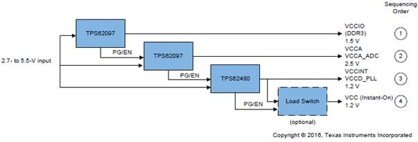
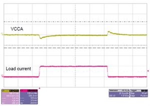
The reference design supports the dual-supply power option of the MAX 10 and contains an option which supports the Instant-On feature. The power supply supports a 6-A VCC (core) rail with the TPS62480 step-down converter and provides 2-A each for the VCCIO (for double data rate (DDR) memory) and VCCA (analog) rails with two TPS62097 step-down converters. These characteristics enable you to take advantage of the full operating performance of the FPGA and not be design-constrained by any power supply limits. The design guide contains all the necessary data and waveforms to meet the FPGA power requirements. Figure 1 shows an example of the VCCA rail meeting the 5% regulation requirement to a 50% load step with plenty of margin.
 Figure 1 VCCA Transient Response to a
50% Load Step
Figure 1 VCCA Transient Response to a
50% Load StepNow that the power supply is proven to support the FPGA, how efficient and small is it? The reference design fits all three power supply rails in less than 300 mm2 of PCB space. While a smaller size is possible by using power modules, 300 mm2 is already a very small size for a discrete design that requires three different voltages.
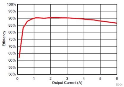
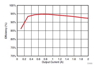
Efficiency is important at the power supply’s full rated load but also at your full load, which may be less than the power supply’s rated current based on which FPGA functionality is used. A flat efficiency curve is important to get high efficiency at a variety of load currents. Overall for all rails combined, the TIDA-01366 achieves 89% efficiency at its full load current, but more importantly achieves 92% efficiency at half load. Figure 2 shows the efficiency of the VCC rail, which peaks at 91%. Figure 3 shows the efficiency of the VCCA rail, which peaks at 95%.
 Figure 2 VCC Efficiency with a 5-v
Input Voltage
 Figure 3 VCCA Efficiency with a 5-v
Input Voltage
Figure 3 VCCA Efficiency with a 5-v
Input VoltageHigh efficiency also supports operation at higher ambient temperatures. The reference design uses components which are rated to operate at 125°C. Additionally, the design includes a temperature warning flag which asserts at 120°C for an extra layer of safety. If asserted, the system then takes actions to reduce its power consumption, such as reducing the FPGA’s activity, or to decrease the system temperature, such as turning on a fan.
Small, efficient, and proven.
IMPORTANT NOTICE AND DISCLAIMER
TI PROVIDES TECHNICAL AND RELIABILITY DATA (INCLUDING DATASHEETS), DESIGN RESOURCES (INCLUDING REFERENCE DESIGNS), APPLICATION OR OTHER DESIGN ADVICE, WEB TOOLS, SAFETY INFORMATION, AND OTHER RESOURCES “AS IS” AND WITH ALL FAULTS, AND DISCLAIMS ALL WARRANTIES, EXPRESS AND IMPLIED, INCLUDING WITHOUT LIMITATION ANY IMPLIED WARRANTIES OF MERCHANTABILITY, FITNESS FOR A PARTICULAR PURPOSE OR NON-INFRINGEMENT OF THIRD PARTY INTELLECTUAL PROPERTY RIGHTS.
These resources are intended for skilled developers designing with TI products. You are solely responsible for (1) selecting the appropriate TI products for your application, (2) designing, validating and testing your application, and (3) ensuring your application meets applicable standards, and any other safety, security, or other requirements. These resources are subject to change without notice. TI grants you permission to use these resources only for development of an application that uses the TI products described in the resource. Other reproduction and display of these resources is prohibited. No license is granted to any other TI intellectual property right or to any third party intellectual property right. TI disclaims responsibility for, and you will fully indemnify TI and its representatives against, any claims, damages, costs, losses, and liabilities arising out of your use of these resources.
TI’s products are provided subject to TI’s Terms of Sale (www.ti.com/legal/termsofsale.html) or other applicable terms available either on ti.com or provided in conjunction with such TI products. TI’s provision of these resources does not expand or otherwise alter TI’s applicable warranties or warranty disclaimers for TI products.
Mailing Address: Texas Instruments, Post Office Box 655303, Dallas, Texas 75265
Copyright © 2023, Texas Instruments Incorporated